AD9549/PCBZ Analog Devices Inc, AD9549/PCBZ Datasheet - Page 26
AD9549/PCBZ
Manufacturer Part Number
AD9549/PCBZ
Description
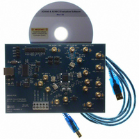
BOARD EVALUATION FOR AD9549
Manufacturer
Analog Devices Inc
Datasheet
1.AD9549ABCPZ.pdf
(76 pages)
Specifications of AD9549/PCBZ
Main Purpose
Timing, Clock Generator
Embedded
No
Utilized Ic / Part
AD9549
Primary Attributes
2 Inputs, 2 Outputs, VCO
Secondary Attributes
CMOS, HSTL Output Logic, Graphical User Interface
Lead Free Status / RoHS Status
Lead free / RoHS Compliant


AD9549
For example, if f
quency lock threshold of 1% is specified, the frequency lock
detect threshold value is
Hence, 170,667 (0x00029AAB) is the value that should be stored
in the frequency lock detect threshold bits.
The duration of the frequency lock/unlock detection process is
controlled in exactly the same way as the phase lock/unlock
detection process in the previous section. However, different
control registers are used: namely, the frequency lock/unlock
watchdog timer bits.
REFERENCE MONITORS
Loss of Reference
The AD9549 can set an alert when one or both of the reference
signals are not present. Each of the two reference inputs (REFA,
REFB) has a dedicated LOR (loss of reference) circuit enabled
via the I/O register map. Detection of an LOR condition sets the
appropriate LOR bit in both a status register and an IRQ status
register in the I/O register map. The LOR state is also internally
available to the multipurpose status pins (S1 to S4) of the AD9549.
By setting the appropriate bit in the I/O register map, the user
can assign a status pin to each of the LOR flags. This provides
a means to control external hardware based on the state of the
LOR flags directly.
The LOR circuits are internal watchdog timers that have a
programmable period. The period of the timer is set via the
I/O register map so that its period is longer than that of the
monitored reference signal. The rising edge of the reference
signal continuously resets the watchdog timer. If the timer
reaches a full count, this indicates that the reference was either
lost or its period was longer than the timer period. LOR does not
differentiate between these.
The period for each of the LOR timers is controlled by a 16-bit
word in the I/O register map. The period of the timer clock (t
is 2/f
where N is the value of the 16-bit word stored in the I/O register
map for the appropriate LOR circuit.
Choose the value of N so that the watchdog period is greater
than the input reference period, expressed mathematically as
where f
The value of N results in establishing two frequencies: one for
which the LOR signal is never triggered (f
which the LOR signal is always active (f
quencies, the LOR signal intermittently toggles between states.
t
S
round
N
WD
. Therefore, the period of the watchdog timer (t
FLDT
R
>
= (2/f
is the frequency of the input reference.
floor
=
(
1
S
%
)N
R
×
2
= 3 MHz, R = 5, FPFD_Gain = 200, and a fre-
f
3
f
S
R
×
10
6
)
×
2
10
×
10
7
×
200
LOST
×
PRESENT
). Using these fre-
3
×
5
), and one for
10
6
WD
2
=
) is
170
CLK
Rev. D | Page 26 of 76
,
667
)
The values of the two frequency bounds are
Note that when N is chosen to be
the LOR circuit is capable of indicating an LOR condition in
little more than a single input reference period. For example,
if f
value is
This yields the following values for f
Note that N should be chosen sufficiently large to account for
any acceptable deviation in the period of the input reference
signal.
Notice that the value of N is inversely proportional to the
reference frequency, meaning that as the reference frequency
goes up, the precision for adjusting the threshold goes down.
Proper operation of the LOR circuit requires that N be no less
than 3. Therefore, the highest reference frequency for which the
LOR circuit functions properly is given by
Reference Frequency Monitor
The AD9549 can set an alert whenever one or both of the
reference inputs drift in frequency beyond user-specified limits.
Each of the two references has a dedicated out of limits (OOL)
circuit enabled/disabled via the I/O register map. Detection of
an OOL condition sets the appropriate OOL bit in both a status
register and an IRQ status register in the I/O register map. The
user can also assign a status pin (S1 to S4) to each of the OOL
flags by setting the appropriate bit in the I/O register map. This
provides a means to control external hardware based on the
state of the OOL flags directly.
Each reference monitor contains three main building blocks: a
programmable reference divider, a 32-bit counter, and a 32-bit
digital comparator.
S
f
R
= 1 GHz and f
f
f
N
PRESENT
LOST
f
f
f
PRESENT
LOST
LOR[MAX]
MIN
= 2,040,816
DIVIDER
=
16-BIT
=
= 2,049,180
OOL
2
=
floor
f
N
=
S
( 2 −
f
6
R
S
N
GATE
f
= 2.048 MHz, then the smallest usable N
Figure 32. Reference Monitor
S
2
. 2 (
f
) 1
S
048
10
COUNTER
32-BIT
9
×
÷4
10
CLK
6
)
floor
PRESENT
+
LOWER
1
COMPARATOR
LIMIT
2
=
DIGITAL
f
f
and f
S
245
R
UPPER
LIMIT
+
LOST
1
,
:
OOL
Related parts for AD9549/PCBZ
Image
Part Number
Description
Manufacturer
Datasheet
Request
R


Part Number:
Description:
±1.7g Dual-Axis IMEMS Accelerometer Evaluation Board
Manufacturer:
Analog Devices Inc
Datasheet:

Part Number:
Description:
Inertial Sensor Evaluation System
Manufacturer:
Analog Devices Inc
Datasheet:
Part Number:
Description:
Manufacturer:
Analog Devices Inc
Datasheet:
Part Number:
Description:
Manufacturer:
Analog Devices Inc
Datasheet:
Part Number:
Description:
Manufacturer:
Analog Devices Inc
Datasheet:
Part Number:
Description:
Manufacturer:
Analog Devices Inc
Datasheet:
Part Number:
Description:
Manufacturer:
Analog Devices Inc
Datasheet:
Part Number:
Description:
Manufacturer:
Analog Devices Inc
Datasheet:
Part Number:
Description:
Manufacturer:
Analog Devices Inc
Datasheet:
Part Number:
Description:
Manufacturer:
Analog Devices Inc
Datasheet:
Part Number:
Description:
Manufacturer:
Analog Devices Inc
Datasheet:
Part Number:
Description:
Manufacturer:
Analog Devices Inc
Datasheet: