AD9549/PCBZ Analog Devices Inc, AD9549/PCBZ Datasheet - Page 42
AD9549/PCBZ
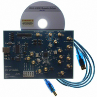
Manufacturer Part Number
AD9549/PCBZ
Description
BOARD EVALUATION FOR AD9549
Manufacturer
Analog Devices Inc
Datasheet
1.AD9549ABCPZ.pdf
(76 pages)
Specifications of AD9549/PCBZ
Main Purpose
Timing, Clock Generator
Embedded
No
Utilized Ic / Part
AD9549
Primary Attributes
2 Inputs, 2 Outputs, VCO
Secondary Attributes
CMOS, HSTL Output Logic, Graphical User Interface
Lead Free Status / RoHS Status
Lead free / RoHS Compliant


AD9549
POWER-UP
POWER-ON RESET
On initial power-up, it is recommended that the user apply a
RESET pulse, at least 75 ns in duration, on Pin 59 after both of
the following two conditions are met:
•
•
The high-to-low transition of the RESET pulse is the active
edge of the pulse and therefore the user is afforded the option
of holding RESET high during power–up.
Less than 1 ns after RESET goes high, the S1 to S4 configuration
pins go high impedance and remain high impedance until RESET
is deactivated. This allows strapping and configuration during
RESET.
Because of this reset sequence, external power supply sequenc-
ing is not critical.
PROGRAMMING SEQUENCE
The following sequence should be used when initializing the
AD9549:
1.
2.
3.
4.
The 3.3 V supply is greater than 2.35 V ± 0.1 V.
The 1.8 V supply is greater than 1.4 V ± 0.05 V.
Apply power. After the power supplies reach a threshold and
stabilize, it is recommended that an active high pulse be
asserted on the RESET pin (Pin 59), initiating a hard reset.
It is important to be sure that the desired configuration
registers have single-tone mode set (Register 0x0100, Bit 5)
and that the close loop bit (Register 0x0100[0]) is cleared.
If the close loop bit is set on initial loading, the AD9549
attempts to lock the loop before it has been configured.
When the registered are loaded, the OOL (out of limits)
and LOR (loss of reference) can be monitored to ensure
that a valid reference signal is present on REFA or REFB.
If a valid reference is present, Register 0x0100 can be
reprogrammed to clear single-tone mode and lock the loop.
Automatic holdover mode can then be used to make the
AD9549 immune to any disturbance on the reference inputs.
Rev. D | Page 42 of 76
Use the following sequence when changing frequencies in the
AD9549:
1.
2.
3.
4.
5.
6.
Note the following:
•
•
•
Open the loop and enter single-tone mode via
Register 0x0100.
Enter the new register settings.
Write 0x1E to Register 0x0012.
When the registers are loaded, the OOL (out of limits) and
LOR (loss of reference) can be monitored to ensure that
a valid reference signal is present on REFA or REFB.
If a valid reference is present, Register 0x0100 can be repro-
grammed to clear single-tone mode and lock the loop.
Automatic holdover mode can then be used to make the
AD9549 immune to any disturbance on the reference
inputs.
Attempting to lock the loop without a valid reference can
put the AD9549 into a state that requires a reset, or at a
minimum, writing 0xFF to Register 0x0012.
Automatic holdover mode is not available unless the loop
has been successfully closed.
If the user desires to open and close the loop manually, it is
recommended that 0x1E to be written to Register 0x0012
prior to closing the loop again.
Related parts for AD9549/PCBZ
Image
Part Number
Description
Manufacturer
Datasheet
Request
R


Part Number:
Description:
±1.7g Dual-Axis IMEMS Accelerometer Evaluation Board
Manufacturer:
Analog Devices Inc
Datasheet:

Part Number:
Description:
Inertial Sensor Evaluation System
Manufacturer:
Analog Devices Inc
Datasheet:
Part Number:
Description:
Manufacturer:
Analog Devices Inc
Datasheet:
Part Number:
Description:
Manufacturer:
Analog Devices Inc
Datasheet:
Part Number:
Description:
Manufacturer:
Analog Devices Inc
Datasheet:
Part Number:
Description:
Manufacturer:
Analog Devices Inc
Datasheet:
Part Number:
Description:
Manufacturer:
Analog Devices Inc
Datasheet:
Part Number:
Description:
Manufacturer:
Analog Devices Inc
Datasheet:
Part Number:
Description:
Manufacturer:
Analog Devices Inc
Datasheet:
Part Number:
Description:
Manufacturer:
Analog Devices Inc
Datasheet:
Part Number:
Description:
Manufacturer:
Analog Devices Inc
Datasheet:
Part Number:
Description:
Manufacturer:
Analog Devices Inc
Datasheet: