AD9549/PCBZ Analog Devices Inc, AD9549/PCBZ Datasheet - Page 33
AD9549/PCBZ
Manufacturer Part Number
AD9549/PCBZ
Description
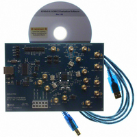
BOARD EVALUATION FOR AD9549
Manufacturer
Analog Devices Inc
Datasheet
1.AD9549ABCPZ.pdf
(76 pages)
Specifications of AD9549/PCBZ
Main Purpose
Timing, Clock Generator
Embedded
No
Utilized Ic / Part
AD9549
Primary Attributes
2 Inputs, 2 Outputs, VCO
Secondary Attributes
CMOS, HSTL Output Logic, Graphical User Interface
Lead Free Status / RoHS Status
Lead free / RoHS Compliant


FDBK_IN INPUTS
The feedback pins, FDBK_IN and FDBK_INB, serve as the input
to the feedback path of the digital PLL. Typically, these pins are
used to receive the signal generated by the DDS after it has been
band-limited by the external reconstruction filter.
A diagram of the FDBK input pins is provided in Figure 40,
which includes some of the internal components used to bias
the input circuitry. Note that the FDBK input pins are internally
biased to a dc level of ~1 V. Care should be taken to ensure that
any external connections do not disturb the dc bias because this
may significantly degrade performance.
REFERENCE INPUTS
Reference Clock Receiver
The reference clock receiver is the point at which the user
supplies the input clock signal that the synchronizer synthesizes
into an output clock. The clock receiver circuit is able to handle
a relatively broad range of input levels as well as frequencies
from 8 kHz up to 750 MHz.
Figure 41 is a diagram of the REFA and REFB input pins, which
includes some of the internal components used to bias the input
circuitry. Note that the REF input pins are internally biased by a
dc source, V
connections do not disturb the dc bias because such a disturbance
may significantly degrade performance.
Note that support for redundant reference clocks is achieved by
using the two reference clock receivers (REFA and REFB).
FDBK_INB
FDBK_IN
CLKMODESEL
B
. Care should be taken to ensure that any external
SYSCLKB
SYSCLK
Figure 40. Differential FDBK Inputs
V
SS
~1pF
~1pF
(I/O REGISTER BIT)
PD SYSCLK PLL
+
~1V
2
15kΩ
15kΩ
ENABLED
SYSCLK
1
0
PLL
2
2
OUTPUT SECTION
~2pF
TO S-DIVIDER
AND CLOCK
SYSCLK PLL BYPASSED
1
0
WITH EXTERNAL DRIVE
2
2
Figure 42. System Clock Generator Block Diagram
V
SS
WITH CRYSTAL
RESONATOR
Rev. D | Page 33 of 76
2× REFERENCE FREQUENCY DOUBLER
1
0
DETECTOR
To accommodate a variety of input signal conditions, the value
of V
Table 6 gives the value of V
Table 6. Setting of Input Bias Voltage (V
Reference Bias Level, Register 0x040F[1:0]
00 (default)
01
10
11
SYSCLK INPUTS
Functional Description
The SYSCLK pins are where an external time base is connected
to the AD9549 for generating the internal high frequency
system clock (f
The SYSCLK inputs can be operated in one of three modes:
•
•
•
A functional diagram of the system clock generator is shown in
Figure 42.
(OR REFB_INB)
BIPOLAR
(OR REFB_IN)
EDGE
(I/O REGISTER BIT)
REFA_INB
B
SYSCLK PLL bypassed
SYSCLK PLL enabled with input signal generated externally
Crystal resonator with SYSCLK PLL enabled
REFA_IN
is programmable via a pair of bits in the I/O register map.
0
1
GND
S
).
LOOP_FILTER
MULTIPLIER
~1pF
~1pF
SYSCLK
Figure 41. Reference Inputs
PLL
1pF
B
for the bit pattern in Register 0x040F.
8kΩ
8kΩ
V
V
2
2
DD
B
+
SWITCHING LOGIC
1
0
TO REFERENCE
MONITOR AND
2
V
SS
B
)
DAC
SAMPLE
CLOCK
V
AVDD3 − 800 mV
AVDD3 − 400 mV
AVDD3 − 1600 mV
AVDD3 − 1200 mV
B
AD9549
Related parts for AD9549/PCBZ
Image
Part Number
Description
Manufacturer
Datasheet
Request
R


Part Number:
Description:
±1.7g Dual-Axis IMEMS Accelerometer Evaluation Board
Manufacturer:
Analog Devices Inc
Datasheet:

Part Number:
Description:
Inertial Sensor Evaluation System
Manufacturer:
Analog Devices Inc
Datasheet:
Part Number:
Description:
Manufacturer:
Analog Devices Inc
Datasheet:
Part Number:
Description:
Manufacturer:
Analog Devices Inc
Datasheet:
Part Number:
Description:
Manufacturer:
Analog Devices Inc
Datasheet:
Part Number:
Description:
Manufacturer:
Analog Devices Inc
Datasheet:
Part Number:
Description:
Manufacturer:
Analog Devices Inc
Datasheet:
Part Number:
Description:
Manufacturer:
Analog Devices Inc
Datasheet:
Part Number:
Description:
Manufacturer:
Analog Devices Inc
Datasheet:
Part Number:
Description:
Manufacturer:
Analog Devices Inc
Datasheet:
Part Number:
Description:
Manufacturer:
Analog Devices Inc
Datasheet:
Part Number:
Description:
Manufacturer:
Analog Devices Inc
Datasheet: