AD9549/PCBZ Analog Devices Inc, AD9549/PCBZ Datasheet - Page 2
AD9549/PCBZ
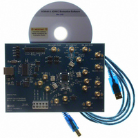
Manufacturer Part Number
AD9549/PCBZ
Description
BOARD EVALUATION FOR AD9549
Manufacturer
Analog Devices Inc
Datasheet
1.AD9549ABCPZ.pdf
(76 pages)
Specifications of AD9549/PCBZ
Main Purpose
Timing, Clock Generator
Embedded
No
Utilized Ic / Part
AD9549
Primary Attributes
2 Inputs, 2 Outputs, VCO
Secondary Attributes
CMOS, HSTL Output Logic, Graphical User Interface
Lead Free Status / RoHS Status
Lead free / RoHS Compliant


AD9549
TABLE OF CONTENTS
Features .............................................................................................. 1
Applications ....................................................................................... 1
General Description ......................................................................... 1
Basic Block Diagram ........................................................................ 1
Revision History ............................................................................... 3
Specifications ..................................................................................... 4
Absolute Maximum Ratings ............................................................ 9
Pin Configuration and Function Descriptions ........................... 10
Typical Performance Characteristics ........................................... 13
Input/Output Termination Recommendations .......................... 16
Theory of Operation ...................................................................... 17
Thermal Performance .................................................................... 41
DC Specifications ......................................................................... 4
AC Specifications .......................................................................... 6
Thermal Resistance ...................................................................... 9
ESD Caution .................................................................................. 9
Overview ...................................................................................... 17
Digital PLL Core (DPLLC)........................................................ 17
Phase Detector ............................................................................ 21
Digital Loop Filter Coefficients ................................................ 22
Closed-Loop Phase Offset ......................................................... 24
Lock Detection ............................................................................ 24
Reference Monitors .................................................................... 26
Reference Switchover ................................................................. 27
Holdover ...................................................................................... 29
Output Frequency Range Control ............................................ 32
Reconstruction Filter ................................................................. 32
FDBK_IN Inputs ........................................................................ 33
Reference Inputs ......................................................................... 33
SYSCLK Inputs ........................................................................... 33
Harmonic Spur Reduction ........................................................ 35
Output Clock Drivers and 2× Frequency Multiplier ............. 36
Frequency Slew Limiter ............................................................. 37
Frequency Estimator .................................................................. 37
Status and Warnings ................................................................... 39
Rev. D | Page 2 of 76
Power-Up ......................................................................................... 42
Power Supply Partitioning ............................................................. 43
Serial Control Port ......................................................................... 44
I/O Register Map ............................................................................ 48
I/O Register Descriptions .............................................................. 53
Applications Information .............................................................. 73
Outline Dimensions ....................................................................... 74
Power-On Reset .......................................................................... 42
Programming Sequence ............................................................ 42
3.3 V Supplies .............................................................................. 43
1.8 V Supplies .............................................................................. 43
Serial Control Port Pin Descriptions ....................................... 44
Operation of Serial Control Port .............................................. 44
The Instruction Word (16 Bits) ................................................ 45
MSB/LSB First Transfers ........................................................... 45
Serial Port Configuration (Register 0x0000 to Register
0x0005) ........................................................................................ 53
Power-Down and Reset (Register 0x0010 to Register 0x0013)
....................................................................................................... 53
System Clock (Register 0x0020 to Register 0x0023) ............. 54
Digital PLL Control and Dividers (Register 0x0100 to
Register 0x0130) ......................................................................... 55
Free-Run (Single-Tone) Mode (Register 0x01A0 to Register
0x01AD) ...................................................................................... 61
Reference Selector/Holdover (Register 0x01C0 to Register
0x01C3) ........................................................................................ 62
Doubler and Output Drivers (Register 0x0200 to Register
0x0201) ........................................................................................ 63
Monitor (Register 0x0300 to Register 0x0335)....................... 64
Calibration (User-Accessible Trim) (Register 0x0400 to
Register 0x0410) ......................................................................... 70
Harmonic Spur Reduction (Register 0x0500 to Register
0x0509) ........................................................................................ 71
Sample Applications Circuit ..................................................... 73
Ordering Guide .......................................................................... 74
Related parts for AD9549/PCBZ
Image
Part Number
Description
Manufacturer
Datasheet
Request
R


Part Number:
Description:
±1.7g Dual-Axis IMEMS Accelerometer Evaluation Board
Manufacturer:
Analog Devices Inc
Datasheet:

Part Number:
Description:
Inertial Sensor Evaluation System
Manufacturer:
Analog Devices Inc
Datasheet:
Part Number:
Description:
Manufacturer:
Analog Devices Inc
Datasheet:
Part Number:
Description:
Manufacturer:
Analog Devices Inc
Datasheet:
Part Number:
Description:
Manufacturer:
Analog Devices Inc
Datasheet:
Part Number:
Description:
Manufacturer:
Analog Devices Inc
Datasheet:
Part Number:
Description:
Manufacturer:
Analog Devices Inc
Datasheet:
Part Number:
Description:
Manufacturer:
Analog Devices Inc
Datasheet:
Part Number:
Description:
Manufacturer:
Analog Devices Inc
Datasheet:
Part Number:
Description:
Manufacturer:
Analog Devices Inc
Datasheet:
Part Number:
Description:
Manufacturer:
Analog Devices Inc
Datasheet:
Part Number:
Description:
Manufacturer:
Analog Devices Inc
Datasheet: