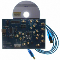
AD9549/PCBZ Analog Devices Inc, AD9549/PCBZ Datasheet - Page 32
AD9549/PCBZ
Manufacturer Part Number
AD9549/PCBZ
Description
BOARD EVALUATION FOR AD9549
Manufacturer
Analog Devices Inc
Datasheet
1.AD9549ABCPZ.pdf
(76 pages)
Specifications of AD9549/PCBZ
Main Purpose
Timing, Clock Generator
Embedded
No
Utilized Ic / Part
AD9549
Primary Attributes
2 Inputs, 2 Outputs, VCO
Secondary Attributes
CMOS, HSTL Output Logic, Graphical User Interface
Lead Free Status / RoHS Status
Lead free / RoHS Compliant


AD9549
OUTPUT FREQUENCY RANGE CONTROL
Under normal operating conditions, the output frequency is
dynamically changing in response to the output of the digital
loop filter. The loop filter can steer the DDS to any frequency
between dc and f
is given the option of placing limits on the tuning range of the
DDS via two 48-bit registers in the I/O register map: the FTW
upper limit and the FTW lower limit. If the tuning word input
exceeds the upper or lower frequency limit boundaries, the
tuning word is clipped to the appropriate value. The default
setting for these registers is f
frequency word tuning limits should be used with caution
because they may make the digital loop unstable.
It may be desirable to limit the output range of the DDS to a
narrow band of frequencies (for example, to achieve better jitter
performance in conjunction with a band pass filter). See the Use
of Narrow-Band Filter for High Performance section for more
information about this feature.
RECONSTRUCTION FILTER
The origin of the output clock signal produced by the AD9549 is
the combined DDS and DAC. The DAC output signal appears as
a sinusoid sampled at f
mined by the frequency tuning word (FTW) that appears at the
input to the DDS. The DAC output is typically passed through
an external reconstruction filter that serves to remove the
REF IN
REF IN
Figure 38. Application of the Frequency Limiter
÷R
÷R
S
/2 (with 48-bit resolution). However, the user
÷S
÷S
DETECTOR
DETECTOR
PHASE
PHASE
S
. The frequency of the sinusoid is deter-
S
/2 and dc, respectively. The
MAGNITUDE
–100
–20
–40
–60
–80
0
(dB)
FILTER
FILTER
LOOP
LOOP
BASE BAND
IMAGE 0
PRIMARY
SPURS
RECONSTRUCTION
RECONSTRUCTION
SIGNAL
BAND PASS
EXTERNAL
EXTERNAL
LOW PASS
FREQUENCY
FILTER
FILTER
Figure 39. DAC Spectrum vs. Reconstruction Filter Response
LIMITER
DDS/DAC
DDS/DAC
f
s
/2
RESPONSE
FILTER
IMAGE 1
Rev. D | Page 32 of 76
f
s
IMAGE 2
3
f
artifacts of the sampling process and other spurs outside the
filter bandwidth. The signal is then brought back on-chip to
be converted to a square wave that is routed internally to the
output clock driver or the 2× DLL multiplier.
Because the DAC constitutes a sampled system, its output must
be filtered so that the analog waveform accurately represents the
digital samples supplied to the DAC input. The unfiltered DAC
output contains the desired baseband signal, which extends from
dc to the Nyquist frequency (f
baseband signal that theoretically extend to infinity. Note that
the odd images (shown in Figure 39) are mirror images of the
baseband signal. Furthermore, the entire DAC output spectrum
is affected by a sin(x)/x response, which is caused by the sample-
and-hold nature of the DAC output signal.
The response of the reconstruction filter should preserve the
baseband signal (Image 0), while completely rejecting all other
images. However, a practical filter implementation typically
exhibits a relatively flat pass band that covers the desired output
frequency plus 20%, rolls off as steeply as possible, and then
maintains significant (though not complete) rejection of the
remaining images.
Because the DAC output signal serves as the feedback signal for
the digital PLL, the design of the reconstruction filter can have
a significant impact on the overall jitter performance. Hence,
good filter design and implementation techniques are important
for obtaining the best possible jitter results.
Use of Narrow-Band Filter for High Performance
A distinct advantage of the AD9549 architecture is its ability to
constrain the frequency output range of the DDS. This allows
the user to employ a narrow-band reconstruction filter instead
of the low-pass response shown in Figure 39, resulting in less
jitter on the output. For example, suppose that the nominal
output frequency of the DDS is 150 MHz. One might then
choose a 5 MHz narrow band filter centered at 150 MHz. By
using the AD9549's DDS frequency limiting feature, the user
can constrain the output frequency to 150 MHz ± 4.9 MHz
(which allows for a 100 kHz margin at the pass-band edges).
This ensures that a feedback signal is always present for the
digital PLL. Such a design is extremely difficult to implement
with conventional PLL architectures.
s
/2
ENVELOPE
SIN(x)/x
IMAGE 3
2
f
s
IMAGE 4
5
f
s
/2
S
/2). It also contains images of the
f
Related parts for AD9549/PCBZ
Image
Part Number
Description
Manufacturer
Datasheet
Request
R


Part Number:
Description:
±1.7g Dual-Axis IMEMS Accelerometer Evaluation Board
Manufacturer:
Analog Devices Inc
Datasheet:

Part Number:
Description:
Inertial Sensor Evaluation System
Manufacturer:
Analog Devices Inc
Datasheet:
Part Number:
Description:
Manufacturer:
Analog Devices Inc
Datasheet:
Part Number:
Description:
Manufacturer:
Analog Devices Inc
Datasheet:
Part Number:
Description:
Manufacturer:
Analog Devices Inc
Datasheet:
Part Number:
Description:
Manufacturer:
Analog Devices Inc
Datasheet:
Part Number:
Description:
Manufacturer:
Analog Devices Inc
Datasheet:
Part Number:
Description:
Manufacturer:
Analog Devices Inc
Datasheet:
Part Number:
Description:
Manufacturer:
Analog Devices Inc
Datasheet:
Part Number:
Description:
Manufacturer:
Analog Devices Inc
Datasheet:
Part Number:
Description:
Manufacturer:
Analog Devices Inc
Datasheet:
Part Number:
Description:
Manufacturer:
Analog Devices Inc
Datasheet: