AD9549/PCBZ Analog Devices Inc, AD9549/PCBZ Datasheet - Page 37
AD9549/PCBZ
Manufacturer Part Number
AD9549/PCBZ
Description
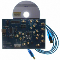
BOARD EVALUATION FOR AD9549
Manufacturer
Analog Devices Inc
Datasheet
1.AD9549ABCPZ.pdf
(76 pages)
Specifications of AD9549/PCBZ
Main Purpose
Timing, Clock Generator
Embedded
No
Utilized Ic / Part
AD9549
Primary Attributes
2 Inputs, 2 Outputs, VCO
Secondary Attributes
CMOS, HSTL Output Logic, Graphical User Interface
Lead Free Status / RoHS Status
Lead free / RoHS Compliant


Single-Ended CMOS Output
In addition to the high speed differential output clock driver, the
AD9549 provides an independent, single-ended output, CMOS
clock driver. It serves as a relatively low speed (<150 MHz) clock
source. The origin of the signal generated by the CMOS clock
driver is determined by the appropriate control bits in the I/O
register map. The user can select one of two sources under
program control.
One source is the signal generated by the DDS after it has been
externally filtered and brought back on chip. In this configura-
tion, the CMOS clock driver generates the same frequency as
appears at the output of the DDS.
Note that in this configuration, the DDS output frequency must
not exceed 50 MHz.
The other source is the output of the feedback divider (S-divider).
In this configuration, the CMOS clock driver generates the same
frequency as the input reference after optional prescaling by the
R-divider (that is, f
a maximum of 25 MHz.
FREQUENCY SLEW LIMITER
The frequency slew limiting capability enables users to specify the
maximum rate of frequency change that appears at the output.
The function is programmable via the I/O register map. Program
control a bit to enable/disable the function (the default condition
is disable) and a register that sets the desired slew rate.
The frequency slew limiter is located between the digital loop
filter and the CCI filter, as shown in Figure 47.
The frequency slew limiter sets a boundary on the rate of change of
the output frequency of the DDS. The frequency slew limiting
constant, K
The value of the constant is determined by
where:
P
f
δf/δt is the desired frequency slew rate limitation.
S
IO
is the DAC sample rate.
is the value stored in the I/O register map for the P-divider.
K
SLEW
SLEW
round
, is a 48-bit value stored in the I/O register map.
CMOS
= f
2
48
f
R
S
/R), which is inherently limited to
2
P
IO
REF IN
δf
δt
÷R
CONVERTER
DETECTOR)
FROM “S”-DIVIDER
DIGITAL
(PHASE
TIME
TO
Figure 47. Frequency Slew Limiter
DIGITAL
FILTER
Rev. D | Page 37 of 76
LOOP
FREQUENCY
LIMITER
For example, if f
The resulting slew rate can be calculated as
The preceding example yields δf/δt = 5.003 kHz/sec.
FREQUENCY ESTIMATOR
The frequency estimation function automatically sets the DDS
output frequency so that the feedback frequency (f
prescaled reference frequency (f
error tolerance (ε
quickly lock when the reference frequency is not known. The error
tolerance is defined as a fractional error and is controlled by
a 16-bit programmable value (K) via the I/O register map.
The precision of any frequency measurement is dependent on
the following two factors:
The frequency estimator uses f
δt = 1/f
duration of the measurement is controlled by K, which establishes
a measurement interval that is K cycles of the measured signal
such that T
The frequency estimator uses a 17-bit counter to accumulate the
number of δt periods within the measurement interval. The finite
capacity of the counter puts an upper limit on the duration of the
measurement, which is constrained to T
this equates to ~131 μs. The fact that the measurement time is
bounded by T
(K
The value of K
where:
R is the modulus of the feedforward divider.
f
VALUE
SLEW
SLEW
ρ
R
LIMIT
δ
f/
is the input reference frequency.
MAX
δ
t
The timing resolution of the measurement device (δt)
The duration of the measurement (T
K
K
δf
δt
f
) that can be used without causing the counter to overflow.
f
MAX
S
R
SLEW
R
S
FREQUENCY
SLEW LIMIT
(that is, δt = 1 ns for a 1 GHz DAC sample rate). The
ENABLE
= floor
K
meas
0
1
SLEW
round
max
MAX
= KR/f
S
0
). Its primary purpose is to allow the PLL to
means there is a limit to the largest value of K
= 1 GHz, P
is given by
SYSCLK
65
FILTER
2
CCI
48
÷P
f
,
ρ
REF_IN
535
S
(
2
2
P
10
IO
48
9
.
9
)
2
TO
DDS
IO
5 (
= 9, and δf/δt = 5 kHz/sec, then
S
REF_IN
as its measurement reference, so
10
/R) are matched within an
3
max
= 721
= 2
meas
17
)
/f
S
. If f
DDS
/S) and the
S
AD9549
= 1 GHz,
Related parts for AD9549/PCBZ
Image
Part Number
Description
Manufacturer
Datasheet
Request
R


Part Number:
Description:
±1.7g Dual-Axis IMEMS Accelerometer Evaluation Board
Manufacturer:
Analog Devices Inc
Datasheet:

Part Number:
Description:
Inertial Sensor Evaluation System
Manufacturer:
Analog Devices Inc
Datasheet:
Part Number:
Description:
Manufacturer:
Analog Devices Inc
Datasheet:
Part Number:
Description:
Manufacturer:
Analog Devices Inc
Datasheet:
Part Number:
Description:
Manufacturer:
Analog Devices Inc
Datasheet:
Part Number:
Description:
Manufacturer:
Analog Devices Inc
Datasheet:
Part Number:
Description:
Manufacturer:
Analog Devices Inc
Datasheet:
Part Number:
Description:
Manufacturer:
Analog Devices Inc
Datasheet:
Part Number:
Description:
Manufacturer:
Analog Devices Inc
Datasheet:
Part Number:
Description:
Manufacturer:
Analog Devices Inc
Datasheet:
Part Number:
Description:
Manufacturer:
Analog Devices Inc
Datasheet:
Part Number:
Description:
Manufacturer:
Analog Devices Inc
Datasheet: