AD9549/PCBZ Analog Devices Inc, AD9549/PCBZ Datasheet - Page 11
AD9549/PCBZ
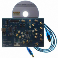
Manufacturer Part Number
AD9549/PCBZ
Description
BOARD EVALUATION FOR AD9549
Manufacturer
Analog Devices Inc
Datasheet
1.AD9549ABCPZ.pdf
(76 pages)
Specifications of AD9549/PCBZ
Main Purpose
Timing, Clock Generator
Embedded
No
Utilized Ic / Part
AD9549
Primary Attributes
2 Inputs, 2 Outputs, VCO
Secondary Attributes
CMOS, HSTL Output Logic, Graphical User Interface
Lead Free Status / RoHS Status
Lead free / RoHS Compliant


Pin No.
20, 21
22
27
28
31
32
33, 39, 43, 52
34
35
37
38
40
41
48
50
51
56
57
58
59
Input/
Output
O
O
I
I
O
I
O
O
O
I
O
I
I
O
O
O
I/O
I/O
I
I
Pin Type
Current set
resistor
Differential
input
Differential
input
1.8 V CMOS
GND
1.8 V HSTL
1.8 V HSTL
Power
3.3 V CMOS
Differential
input
Differential
input
Current set
resistor
Differential
output
Differential
output
3.3 V CMOS
3.3 V CMOS
3.3 V CMOS
3.3 V CMOS
Mnemonic
PFD_VRB,
PFD_VRT
PFD_RSET
SYSCLK
SYSCLKB
LOOP_FILTER
CLKMODESEL
AVSS
OUTB
OUT
AVDD3
OUT_CMOS
FDBK_INB
FDBK_IN
DAC_RSET
DAC_OUT
DAC_OUTB
REFSELECT
HOLDOVER
PWRDOWN
RESET
Rev. D | Page 11 of 76
Description
These pins must be capacitively decoupled. See the Phase Detector Pin
Connections section for details.
Connect a 5 kΩ resistor from this pin to ground (see the Phase Detector Pin
Connections section).
System Clock Input. The system clock input has internal dc biasing and should
always be ac-coupled, except when using a crystal. Single-ended 1.8 V CMOS
can also be used, but it may introduce a spur caused by an input duty cycle
that is not 50%. When using a crystal, tie the CLKMODESEL pin to AVSS, and
connect crystal directly to this pin and Pin 28.
Complementary System Clock. Complementary signal to the input provided
on Pin 27. Use a 0.01 μF capacitor to ground on this pin if the signal provided
on Pin 27 is single-ended.
System Clock Multiplier Loop Filter. When using the frequency multiplier to
drive the system clock, an external loop filter must be constructed and attached to
this pin. This pin should be pulled down to ground with a 1 kΩ resistor when
the system clock PLL is bypassed. See Figure 44 for a diagram of the system
clock PLL loop filter.
Clock Mode Select. Set to GND when connecting a crystal to the system clock
input (Pin 27 and Pin 28). Pull up to 1.8 V when using either an oscillator or an
external clock source. This pin can be left floating when the system clock PLL is
bypassed. (See the SYSCLK Inputs section for details on the use of this pin.)
Analog Ground. Connect to ground.
Complementary HSTL Output. See the Specifications and Primary 1.8 V
Differential HSTL Driver sections for details.
HSTL Output. See the Specifications and Primary 1.8 V Differential HSTL Driver
sections for details.
Analog Supply for CMOS Output Driver. This pin is normally 3.3 V but can be
1.8 V. This pin should be powered even if the CMOS driver is not used. See the
Power Supply Partitioning section for power supply partitioning.
CMOS Output. See the Specifications and the Output Clock Drivers and 2×
Frequency Multiplier sections. This pin is 1.8 V CMOS if Pin 37 is set to 1.8 V.
Complementary Feedback Input. In standard operating mode, this pin is
connected to the filtered DAC_OUTB output. This internally biased input is
typically ac-coupled, and when configured as such, can accept any differential
signal whose single-ended swing is at least 400 mV.
Feedback Input. In standard operating mode, this pin is connected to the
filtered DAC_OUT output.
DAC Output Current Setting Resistor. Connect a resistor (usually 10 kΩ) from
this pin to GND. See the DAC Output section.
DAC Output. This signal should be filtered and sent back on chip through
FDBK_IN input. This pin has an internal 50 Ω pull-down resistor.
Complementary DAC Output. This signal should be filtered and sent back on
chip through FDBK_INB input. This pin has an internal 50 Ω pull-down resistor.
Reference Select Input. In manual mode, the REFSELECT pin operates as a high
impedance input pin; and in automatic mode, it operates as a low impedance
output pin. Logic 0 (low) indicates/selects REFA. Logic 1 (high) indicates/selects
REFB. There is no internal pull-up/pull-down resistor on this pin.
Holdover (Active High). In manual holdover mode, this pin is used to force the
AD9549 into holdover mode. In automatic holdover mode, it indicates
holdover status. There is no internal pull-up/pull-down resistor on this pin.
Power-Down. When this active high pin is asserted, the device becomes
inactive and enters the full power-down state. This pin has an internal 50 kΩ
pull-down resistor.
Chip Reset. When this active high pin is asserted, the chip goes into reset. Note
that on power-up, it is recommended that the user assert a high to low edge
after the power supplies reach a threshold and stabilize. This pin has an
internal 50 kΩ pull-down resistor.
AD9549
Related parts for AD9549/PCBZ
Image
Part Number
Description
Manufacturer
Datasheet
Request
R


Part Number:
Description:
±1.7g Dual-Axis IMEMS Accelerometer Evaluation Board
Manufacturer:
Analog Devices Inc
Datasheet:

Part Number:
Description:
Inertial Sensor Evaluation System
Manufacturer:
Analog Devices Inc
Datasheet:
Part Number:
Description:
Manufacturer:
Analog Devices Inc
Datasheet:
Part Number:
Description:
Manufacturer:
Analog Devices Inc
Datasheet:
Part Number:
Description:
Manufacturer:
Analog Devices Inc
Datasheet:
Part Number:
Description:
Manufacturer:
Analog Devices Inc
Datasheet:
Part Number:
Description:
Manufacturer:
Analog Devices Inc
Datasheet:
Part Number:
Description:
Manufacturer:
Analog Devices Inc
Datasheet:
Part Number:
Description:
Manufacturer:
Analog Devices Inc
Datasheet:
Part Number:
Description:
Manufacturer:
Analog Devices Inc
Datasheet:
Part Number:
Description:
Manufacturer:
Analog Devices Inc
Datasheet:
Part Number:
Description:
Manufacturer:
Analog Devices Inc
Datasheet: