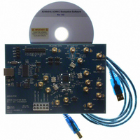
AD9549/PCBZ Analog Devices Inc, AD9549/PCBZ Datasheet - Page 21

AD9549/PCBZ
Manufacturer Part Number
AD9549/PCBZ
Description
BOARD EVALUATION FOR AD9549
Manufacturer
Analog Devices Inc
Datasheet
1.AD9549ABCPZ.pdf
(76 pages)
Specifications of AD9549/PCBZ
Main Purpose
Timing, Clock Generator
Embedded
No
Utilized Ic / Part
AD9549
Primary Attributes
2 Inputs, 2 Outputs, VCO
Secondary Attributes
CMOS, HSTL Output Logic, Graphical User Interface
Lead Free Status / RoHS Status
Lead free / RoHS Compliant
In holdover mode, the AD9549 uses past tuning words when
the loop is closed to determine its output frequency. Therefore,
the loop must be successfully closed for holdover mode to work.
Switching in and out of holdover mode can be either automatic
or manual, depending on register settings.
Typically, the AD9549 operates in closed-loop mode. In closed-
loop mode, the FTW values come from the output of the digital
loop filter and vary with time. The DDS frequency is steered in
a manner similar to a conventional VCO-based PLL.
Note that in closed-loop mode, the DDS phase offset capability
is inoperative.
DAC Output
The output of the digital core of the DDS is a time series of
numbers representing a sinusoidal waveform. This series is
translated to an analog signal by means of a digital-to-analog
converter (DAC).
The DAC outputs its signal to two pins driven by a balanced
current source architecture (see the DAC output diagram in
Figure 26). The peak output current derives from the combi-
nation of two factors. The first is a reference current (I
established at the DAC_RSET pin, and the second is a scale
factor programmed into the I/O register map.
The value of I
between the DAC_RSET pin and ground. The DAC_RSET pin
is internally connected to a virtual voltage reference of 1.2 V
nominal, so the reference current can be calculated by
Note that the recommended value of I
leads to a recommended value for R
The scale factor consists of a 10-bit binary number (FSC)
programmed into the DAC full-scale current register (Address
0x040B and Address 0x040C) in the I/O register map. The full-
scale DAC output current (I
I
I
I
DAC
DAC
FS
/2 + I
_
_
REF
FS
CODE
DAC_REF
CURRENT
=
SWITCH
ARRAY
=
I
DAC
R
DAC
is set by connecting a resistor (R
Figure 26. DAC Output Pins
1
_
51
I
2 .
FS
REF
_
50Ω
IOUT
/2
REF
72
CONTROL
SWITCH
DAC_FS
AVDD3
CODE
AVSS
+
49
52
192
I
IOUTB
FS
) is given by
1024
FSC
50Ω
DAC_REF
I
FS
DAC_REF
/2
50
CURRENT
SWITCH
ARRAY
of 10 kΩ.
is 120 μA, which
I
FS
/2 – I
CODE
DAC_REF
DAC_REF
)
Rev. D | Page 21 of 76
)
Using the recommended value of R
output current can be set with 10-bit granularity over a range of
approximately 8.6 mA to 31.7 mA. The default value is 20 mA.
PHASE DETECTOR
Coarse Phase Detector
The coarse phase detector uses the DAC sample rate (f
determine the edge timing deviation between the REF signal
and the feedback signal generated by the DDS. Hence, f
the timing resolution of the coarse phase detector. At the
recommended rate of f
spans a range of over 131 μs (sufficient to accommodate REF
signal frequencies as low as 8 kHz).
The phase gain of the coarse phase detector is controlled via the
I/O registers by means of two numeric entries. The first is a
3-bit, power-of-2 scale factor, PDS. The second is a 6-bit linear
scale factor, PDG.
Fine Phase Detector
The fine phase detector operates on a divided down version
of f
detector is set using a 4-bit word (PFD_Div) in the I/O register
map (Register 0x0023) and is given by
The default value of PFD_Div is 5, so for f
sample rate of the fine phase detector is 50 MHz. The upper
bound on the maximum allowable input frequency to the phase
detector (f
Therefore, f
The fine phase detector uses a proprietary technique to
determine the phase deviation between the REF signal and
feedback signal.
The phase gain of the fine phase detector is controlled by
an 8-bit scale factor (FPFD_Gain) in the I/O register map
(Register 0x0404). The nominal (default) value of FPFD_Gain
is 200 and establishes the phase gain as
S
as its sampling time base. The sample rate of the fine phase
PhaseGain
Fine
PhaseGain
f
PFD
[
MAX
PFD[MAX]
Phase
PFD[MAX]
]
=
CPD
FP
Detector
) is 49% of the sample rate, or
( 8
D
is 25 MHz in the preceding example.
PFD
=
=
R
S
R
f
= 1 GHz, the coarse phase detector
S
_
2 (
f
f
Sample
S
R
Div
10
×
(
2
)
10
PDS
7
+
Rate
)(
DAC_REF
6
f
PDG
FPFD
R
=
, the full-scale DAC
)
S
( 4
= 1 GHz, the default
_
PFD
Gain
f
S
_
)
AD9549
Div
S
) to
S
)
sets


