C8051F040DK Silicon Laboratories Inc, C8051F040DK Datasheet - Page 7
C8051F040DK
Manufacturer Part Number
C8051F040DK
Description
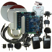
DEV KIT FOR F040/F041/F042/F043
Manufacturer
Silicon Laboratories Inc
Type
MCUr
Specifications of C8051F040DK
Contents
Evaluation Board, Power Supply, USB Cables, Adapter and Documentation
Processor To Be Evaluated
C8051F04x
Interface Type
USB
Silicon Manufacturer
Silicon Labs
Core Architecture
8051
Silicon Core Number
C8051F040
Silicon Family Name
C8051F04x
Lead Free Status / RoHS Status
Contains lead / RoHS non-compliant
For Use With/related Products
Silicon Laboratories C8051 F040, 041, 042, 043 MCUs
Lead Free Status / Rohs Status
Lead free / RoHS Compliant
Other names
336-1205
Available stocks
Company
Part Number
Manufacturer
Quantity
Price
Company:

Part Number:
C8051F040DK
Manufacturer:
SiliconL
Quantity:
9


22. UART1.................................................................................................................... 277
23. Timers.................................................................................................................... 287
24. Programmable Counter Array ............................................................................. 303
25. JTAG (IEEE 1149.1) .............................................................................................. 317
Document Change List............................................................................................. 325
Contact Information.................................................................................................. 326
21.3.Configuration of a Masked Address ............................................................... 271
21.4.Broadcast Addressing .................................................................................... 271
21.5.Frame and Transmission Error Detection....................................................... 272
22.1.Enhanced Baud Rate Generation................................................................... 278
22.2.Operational Modes ......................................................................................... 279
22.3.Multiprocessor Communications .................................................................... 281
23.1.Timer 0 and Timer 1 ....................................................................................... 287
23.2.Timer 2, Timer 3, and Timer 4 ........................................................................ 295
24.1.PCA Counter/Timer ........................................................................................ 304
24.2.Capture/Compare Modules ............................................................................ 305
24.3.Register Descriptions for PCA0...................................................................... 312
25.1.Boundary Scan ............................................................................................... 318
25.2.Flash Programming Commands..................................................................... 321
25.3.Debug Support ............................................................................................... 324
22.2.1.8-Bit UART ............................................................................................. 279
22.2.2.9-Bit UART ............................................................................................. 280
23.1.1.Mode 0: 13-bit Counter/Timer ................................................................ 287
23.1.2.Mode 1: 16-bit Counter/Timer ................................................................ 288
23.1.3.Mode 2: 8-bit Counter/Timer with Auto-Reload...................................... 289
23.1.4.Mode 3: Two 8-bit Counter/Timers (Timer 0 Only)................................. 290
23.2.1.Configuring Timer 2, 3, and 4 to Count Down........................................ 295
23.2.2.Capture Mode ........................................................................................ 296
23.2.3.Auto-Reload Mode ................................................................................. 297
23.2.4.Toggle Output Mode .............................................................................. 298
24.2.1.Edge-triggered Capture Mode................................................................ 306
24.2.2.Software Timer (Compare) Mode........................................................... 307
24.2.3.High-Speed Output Mode ...................................................................... 308
24.2.4.Frequency Output Mode ........................................................................ 309
24.2.5.8-Bit Pulse Width Modulator Mode......................................................... 310
24.2.6.16-Bit Pulse Width Modulator Mode....................................................... 311
25.1.1.EXTEST Instruction................................................................................ 319
25.1.2.SAMPLE Instruction ............................................................................... 319
25.1.3.BYPASS Instruction ............................................................................... 319
25.1.4.IDCODE Instruction................................................................................ 319
Rev. 1.5
C8051F040/1/2/3/4/5/6/7
7
Related parts for C8051F040DK
Image
Part Number
Description
Manufacturer
Datasheet
Request
R

Part Number:
Description:
SMD/C°/SINGLE-ENDED OUTPUT SILICON OSCILLATOR
Manufacturer:
Silicon Laboratories Inc
Part Number:
Description:
Manufacturer:
Silicon Laboratories Inc
Datasheet:
Part Number:
Description:
N/A N/A/SI4010 AES KEYFOB DEMO WITH LCD RX
Manufacturer:
Silicon Laboratories Inc
Datasheet:
Part Number:
Description:
N/A N/A/SI4010 SIMPLIFIED KEY FOB DEMO WITH LED RX
Manufacturer:
Silicon Laboratories Inc
Datasheet:
Part Number:
Description:
N/A/-40 TO 85 OC/EZLINK MODULE; F930/4432 HIGH BAND (REV E/B1)
Manufacturer:
Silicon Laboratories Inc
Part Number:
Description:
EZLink Module; F930/4432 Low Band (rev e/B1)
Manufacturer:
Silicon Laboratories Inc
Part Number:
Description:
I°/4460 10 DBM RADIO TEST CARD 434 MHZ
Manufacturer:
Silicon Laboratories Inc
Part Number:
Description:
I°/4461 14 DBM RADIO TEST CARD 868 MHZ
Manufacturer:
Silicon Laboratories Inc
Part Number:
Description:
I°/4463 20 DBM RFSWITCH RADIO TEST CARD 460 MHZ
Manufacturer:
Silicon Laboratories Inc
Part Number:
Description:
I°/4463 20 DBM RADIO TEST CARD 868 MHZ
Manufacturer:
Silicon Laboratories Inc
Part Number:
Description:
I°/4463 27 DBM RADIO TEST CARD 868 MHZ
Manufacturer:
Silicon Laboratories Inc
Part Number:
Description:
I°/4463 SKYWORKS 30 DBM RADIO TEST CARD 915 MHZ
Manufacturer:
Silicon Laboratories Inc
Part Number:
Description:
N/A N/A/-40 TO 85 OC/4463 RFMD 30 DBM RADIO TEST CARD 915 MHZ
Manufacturer:
Silicon Laboratories Inc
Part Number:
Description:
I°/4463 20 DBM RADIO TEST CARD 169 MHZ
Manufacturer:
Silicon Laboratories Inc