C8051F040DK Silicon Laboratories Inc, C8051F040DK Datasheet - Page 38
C8051F040DK
Manufacturer Part Number
C8051F040DK
Description
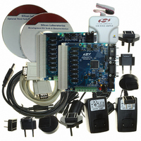
DEV KIT FOR F040/F041/F042/F043
Manufacturer
Silicon Laboratories Inc
Type
MCUr
Specifications of C8051F040DK
Contents
Evaluation Board, Power Supply, USB Cables, Adapter and Documentation
Processor To Be Evaluated
C8051F04x
Interface Type
USB
Silicon Manufacturer
Silicon Labs
Core Architecture
8051
Silicon Core Number
C8051F040
Silicon Family Name
C8051F04x
Lead Free Status / RoHS Status
Contains lead / RoHS non-compliant
For Use With/related Products
Silicon Laboratories C8051 F040, 041, 042, 043 MCUs
Lead Free Status / Rohs Status
Lead free / RoHS Compliant
Other names
336-1205
Available stocks
Company
Part Number
Manufacturer
Quantity
Price
Company:

Part Number:
C8051F040DK
Manufacturer:
SiliconL
Quantity:
9


C8051F040/1/2/3/4/5/6/7
38
P0.5/ALE
P0.7/WR
P0.6/RD
HVAIN+
CANRX
HVCAP
HVREF
CANTX
HVAIN-
AIN0.1
AIN0.2
AIN0.3
Name
DAC0
DAC1
P0.0
P0.1
P0.2
P0.3
P0.4
F040/2/4/6 F041/3/5/7
100
19
20
21
22
23
24
25
99
62
61
60
59
58
57
56
55
Pin Numbers
7
6
Table 4.1. Pin Definitions (Continued)
10
12
13
14
15
16
64
63
55
54
53
52
51
50
49
48
11
2
1
D Out Controller Area Network Transmit Output.
A Out Digital to Analog Converter 0 Voltage Output. (See DAC
A Out Digital to Analog Converter 1 Voltage Output. (See DAC
Type Description
A I/O High Voltage Difference Amplifier Capacitor.
D I/O Port 0.0. See Port Input/Output section for complete
D I/O Port 0.1. See Port Input/Output section for complete
D I/O Port 0.2. See Port Input/Output section for complete
D I/O Port 0.3. See Port Input/Output section for complete
D I/O Port 0.4. See Port Input/Output section for complete
D I/O ALE Strobe for External Memory Address bus (multi-
D I/O /RD Strobe for External Memory Address bus
D I/O /WR Strobe for External Memory Address bus
A In
A In
A In
A In
A In
A In
D In
ADC0 Input Channel 1 (See ADC0 Specification for com-
plete description).
ADC0 Input Channel 2 (See ADC0 Specification for com-
plete description).
ADC0 Input Channel 3 (See ADC0 Specification for com-
plete description).
High Voltage Difference Amplifier Bias Reference.
High Voltage Difference Amplifier Positive Signal Input.
High Voltage Difference Amplifier Negative Signal Input.
Controller Area Network Receive Input.
Specification for complete description). (C8051F040/1/2/3
only)
Specification for complete description). (C8051F040/1/2/3
only)
description.
description.
description.
description.
description.
plexed mode) Port 0.5
See Port Input/Output section for complete description.
Port 0.6
See Port Input/Output section for complete description.
Port 0.7
See Port Input/Output section for complete description.
Rev. 1.5
Related parts for C8051F040DK
Image
Part Number
Description
Manufacturer
Datasheet
Request
R

Part Number:
Description:
SMD/C°/SINGLE-ENDED OUTPUT SILICON OSCILLATOR
Manufacturer:
Silicon Laboratories Inc
Part Number:
Description:
Manufacturer:
Silicon Laboratories Inc
Datasheet:
Part Number:
Description:
N/A N/A/SI4010 AES KEYFOB DEMO WITH LCD RX
Manufacturer:
Silicon Laboratories Inc
Datasheet:
Part Number:
Description:
N/A N/A/SI4010 SIMPLIFIED KEY FOB DEMO WITH LED RX
Manufacturer:
Silicon Laboratories Inc
Datasheet:
Part Number:
Description:
N/A/-40 TO 85 OC/EZLINK MODULE; F930/4432 HIGH BAND (REV E/B1)
Manufacturer:
Silicon Laboratories Inc
Part Number:
Description:
EZLink Module; F930/4432 Low Band (rev e/B1)
Manufacturer:
Silicon Laboratories Inc
Part Number:
Description:
I°/4460 10 DBM RADIO TEST CARD 434 MHZ
Manufacturer:
Silicon Laboratories Inc
Part Number:
Description:
I°/4461 14 DBM RADIO TEST CARD 868 MHZ
Manufacturer:
Silicon Laboratories Inc
Part Number:
Description:
I°/4463 20 DBM RFSWITCH RADIO TEST CARD 460 MHZ
Manufacturer:
Silicon Laboratories Inc
Part Number:
Description:
I°/4463 20 DBM RADIO TEST CARD 868 MHZ
Manufacturer:
Silicon Laboratories Inc
Part Number:
Description:
I°/4463 27 DBM RADIO TEST CARD 868 MHZ
Manufacturer:
Silicon Laboratories Inc
Part Number:
Description:
I°/4463 SKYWORKS 30 DBM RADIO TEST CARD 915 MHZ
Manufacturer:
Silicon Laboratories Inc
Part Number:
Description:
N/A N/A/-40 TO 85 OC/4463 RFMD 30 DBM RADIO TEST CARD 915 MHZ
Manufacturer:
Silicon Laboratories Inc
Part Number:
Description:
I°/4463 20 DBM RADIO TEST CARD 169 MHZ
Manufacturer:
Silicon Laboratories Inc