C8051F040DK Silicon Laboratories Inc, C8051F040DK Datasheet - Page 34
C8051F040DK
Manufacturer Part Number
C8051F040DK
Description
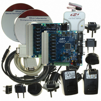
DEV KIT FOR F040/F041/F042/F043
Manufacturer
Silicon Laboratories Inc
Type
MCUr
Specifications of C8051F040DK
Contents
Evaluation Board, Power Supply, USB Cables, Adapter and Documentation
Processor To Be Evaluated
C8051F04x
Interface Type
USB
Silicon Manufacturer
Silicon Labs
Core Architecture
8051
Silicon Core Number
C8051F040
Silicon Family Name
C8051F04x
Lead Free Status / RoHS Status
Contains lead / RoHS non-compliant
For Use With/related Products
Silicon Laboratories C8051 F040, 041, 042, 043 MCUs
Lead Free Status / Rohs Status
Lead free / RoHS Compliant
Other names
336-1205
Available stocks
Company
Part Number
Manufacturer
Quantity
Price
Company:

Part Number:
C8051F040DK
Manufacturer:
SiliconL
Quantity:
9


C8051F040/1/2/3/4/5/6/7
1.10. Comparators and DACs
Each C8051F040/1/2/3 MCU has two 12-bit DACs, and all C8051F04x devices have three comparators on
chip. The MCU data and control interface to each comparator and DAC is via the Special Function Regis-
ters. The MCU can place any DAC or comparator in low power shutdown mode.
The comparators have software programmable hysteresis and response time. Each comparator can gen-
erate an interrupt on its rising edge, falling edge, or both; these interrupts are capable of waking up the
MCU from sleep mode. The comparators' output state can also be polled in software. The comparator out-
puts can be programmed to appear on the Port I/O pins via the Crossbar.
The DACs are voltage output mode and include a flexible output scheduling mechanism. This scheduling
mechanism allows DAC output updates to be forced by a software write or a Timer 2, 3, or 4 overflow. The
DAC voltage reference is supplied via the dedicated VREFD input pin on C8051F040/2 devices or via the
internal voltage reference on C8051F041/3 devices. The DACs are especially useful as references for the
comparators or offsets for the differential inputs of the ADC.
34
(C 8051F040/1/2/3 only)
(C 8051F040/1/2/3 only)
(Port I/O )
DAC0
DAC1
CPn+
CPn-
C om parator inputs
Port 2.[7:2]
Figure 1.14. Comparator and DAC Diagram
CPn O utput
+
-
CPn
3 Com parators
VREF
DAC 0
VREF
DAC 1
CRO SSBAR
Rev. 1.5
SFR's
(Data
Cntrl)
and
Interrupt
H andler
C IP-51
and
Related parts for C8051F040DK
Image
Part Number
Description
Manufacturer
Datasheet
Request
R

Part Number:
Description:
SMD/C°/SINGLE-ENDED OUTPUT SILICON OSCILLATOR
Manufacturer:
Silicon Laboratories Inc
Part Number:
Description:
Manufacturer:
Silicon Laboratories Inc
Datasheet:
Part Number:
Description:
N/A N/A/SI4010 AES KEYFOB DEMO WITH LCD RX
Manufacturer:
Silicon Laboratories Inc
Datasheet:
Part Number:
Description:
N/A N/A/SI4010 SIMPLIFIED KEY FOB DEMO WITH LED RX
Manufacturer:
Silicon Laboratories Inc
Datasheet:
Part Number:
Description:
N/A/-40 TO 85 OC/EZLINK MODULE; F930/4432 HIGH BAND (REV E/B1)
Manufacturer:
Silicon Laboratories Inc
Part Number:
Description:
EZLink Module; F930/4432 Low Band (rev e/B1)
Manufacturer:
Silicon Laboratories Inc
Part Number:
Description:
I°/4460 10 DBM RADIO TEST CARD 434 MHZ
Manufacturer:
Silicon Laboratories Inc
Part Number:
Description:
I°/4461 14 DBM RADIO TEST CARD 868 MHZ
Manufacturer:
Silicon Laboratories Inc
Part Number:
Description:
I°/4463 20 DBM RFSWITCH RADIO TEST CARD 460 MHZ
Manufacturer:
Silicon Laboratories Inc
Part Number:
Description:
I°/4463 20 DBM RADIO TEST CARD 868 MHZ
Manufacturer:
Silicon Laboratories Inc
Part Number:
Description:
I°/4463 27 DBM RADIO TEST CARD 868 MHZ
Manufacturer:
Silicon Laboratories Inc
Part Number:
Description:
I°/4463 SKYWORKS 30 DBM RADIO TEST CARD 915 MHZ
Manufacturer:
Silicon Laboratories Inc
Part Number:
Description:
N/A N/A/-40 TO 85 OC/4463 RFMD 30 DBM RADIO TEST CARD 915 MHZ
Manufacturer:
Silicon Laboratories Inc
Part Number:
Description:
I°/4463 20 DBM RADIO TEST CARD 169 MHZ
Manufacturer:
Silicon Laboratories Inc