C8051F040DK Silicon Laboratories Inc, C8051F040DK Datasheet - Page 11
C8051F040DK
Manufacturer Part Number
C8051F040DK
Description
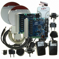
DEV KIT FOR F040/F041/F042/F043
Manufacturer
Silicon Laboratories Inc
Type
MCUr
Specifications of C8051F040DK
Contents
Evaluation Board, Power Supply, USB Cables, Adapter and Documentation
Processor To Be Evaluated
C8051F04x
Interface Type
USB
Silicon Manufacturer
Silicon Labs
Core Architecture
8051
Silicon Core Number
C8051F040
Silicon Family Name
C8051F04x
Lead Free Status / RoHS Status
Contains lead / RoHS non-compliant
For Use With/related Products
Silicon Laboratories C8051 F040, 041, 042, 043 MCUs
Lead Free Status / Rohs Status
Lead free / RoHS Compliant
Other names
336-1205
Available stocks
Company
Part Number
Manufacturer
Quantity
Price
Company:

Part Number:
C8051F040DK
Manufacturer:
SiliconL
Quantity:
9


16. External Data Memory Interface and On-Chip XRAM
17. Port Input/Output
18. Controller Area Network (CAN0)
19. System Management BUS/I
20. Enhanced Serial Peripheral Interface (SPI0)
21. UART0
Figure 16.1. Multiplexed Configuration Example.................................................... 191
Figure 16.2. Non-multiplexed Configuration Example ............................................ 192
Figure 16.3. EMIF Operating Modes ...................................................................... 193
Figure 16.4. Non-multiplexed 16-bit MOVX Timing ................................................ 196
Figure 16.5. Non-multiplexed 8-bit MOVX without Bank Select Timing ................. 197
Figure 16.6. Non-multiplexed 8-bit MOVX with Bank Select Timing ...................... 198
Figure 16.7. Multiplexed 16-bit MOVX Timing........................................................ 199
Figure 16.8. Multiplexed 8-bit MOVX without Bank Select Timing ......................... 200
Figure 16.9. Multiplexed 8-bit MOVX with Bank Select Timing .............................. 201
Figure 17.1. Port I/O Cell Block Diagram ............................................................... 203
Figure 17.2. Port I/O Functional Block Diagram ..................................................... 204
Figure 17.3. Priority Crossbar Decode Table ......................................................... 205
Figure 17.4. Priority Crossbar Decode Table ......................................................... 208
Figure 17.5. Priority Crossbar Decode Table ......................................................... 209
Figure 17.6. Crossbar Example:............................................................................. 211
Figure 18.1. Typical CAN Bus Configuration.......................................................... 227
Figure 18.2. CAN Controller Diagram..................................................................... 228
Figure 18.3. Four Segments of a CAN Bit Time ..................................................... 229
Figure 18.4. CAN0DATH: CAN Data Access Register High Byte .......................... 234
Figure 19.1. SMBus0 Block Diagram ..................................................................... 239
Figure 19.2. Typical SMBus Configuration ............................................................. 240
Figure 19.3. SMBus Transaction ............................................................................ 241
Figure 19.4. Typical Master Transmitter Sequence................................................ 242
Figure 19.5. Typical Master Receiver Sequence.................................................... 243
Figure 19.6. Typical Slave Transmitter Sequence.................................................. 243
Figure 19.7. Typical Slave Receiver Sequence...................................................... 244
Figure 20.1. SPI Block Diagram ............................................................................. 255
Figure 20.2. Multiple-Master Mode Connection Diagram ....................................... 258
Figure 20.3. 3-Wire Single Master and Slave Mode Connection Diagram ............. 258
Figure 20.4. 4-Wire Single Master and Slave Mode Connection Diagram ............. 258
Figure 20.5. Data/Clock Timing Diagram ............................................................... 260
Figure 21.1. UART0 Block Diagram ....................................................................... 265
Figure 21.2. UART0 Mode 0 Timing Diagram ........................................................ 266
Figure 21.3. UART0 Mode 0 Interconnect.............................................................. 267
Figure 21.4. UART0 Mode 1 Timing Diagram ........................................................ 267
Figure 21.5. UART0 Modes 2 and 3 Timing Diagram ............................................ 269
Figure 21.6. UART0 Modes 1, 2, and 3 Interconnect Diagram .............................. 269
Figure 21.7. UART Multi-Processor Mode Interconnect Diagram .......................... 272
2
C BUS (SMBUS0)
Rev. 1.5
C8051F040/1/2/3/4/5/6/7
11
Related parts for C8051F040DK
Image
Part Number
Description
Manufacturer
Datasheet
Request
R

Part Number:
Description:
SMD/C°/SINGLE-ENDED OUTPUT SILICON OSCILLATOR
Manufacturer:
Silicon Laboratories Inc
Part Number:
Description:
Manufacturer:
Silicon Laboratories Inc
Datasheet:
Part Number:
Description:
N/A N/A/SI4010 AES KEYFOB DEMO WITH LCD RX
Manufacturer:
Silicon Laboratories Inc
Datasheet:
Part Number:
Description:
N/A N/A/SI4010 SIMPLIFIED KEY FOB DEMO WITH LED RX
Manufacturer:
Silicon Laboratories Inc
Datasheet:
Part Number:
Description:
N/A/-40 TO 85 OC/EZLINK MODULE; F930/4432 HIGH BAND (REV E/B1)
Manufacturer:
Silicon Laboratories Inc
Part Number:
Description:
EZLink Module; F930/4432 Low Band (rev e/B1)
Manufacturer:
Silicon Laboratories Inc
Part Number:
Description:
I°/4460 10 DBM RADIO TEST CARD 434 MHZ
Manufacturer:
Silicon Laboratories Inc
Part Number:
Description:
I°/4461 14 DBM RADIO TEST CARD 868 MHZ
Manufacturer:
Silicon Laboratories Inc
Part Number:
Description:
I°/4463 20 DBM RFSWITCH RADIO TEST CARD 460 MHZ
Manufacturer:
Silicon Laboratories Inc
Part Number:
Description:
I°/4463 20 DBM RADIO TEST CARD 868 MHZ
Manufacturer:
Silicon Laboratories Inc
Part Number:
Description:
I°/4463 27 DBM RADIO TEST CARD 868 MHZ
Manufacturer:
Silicon Laboratories Inc
Part Number:
Description:
I°/4463 SKYWORKS 30 DBM RADIO TEST CARD 915 MHZ
Manufacturer:
Silicon Laboratories Inc
Part Number:
Description:
N/A N/A/-40 TO 85 OC/4463 RFMD 30 DBM RADIO TEST CARD 915 MHZ
Manufacturer:
Silicon Laboratories Inc
Part Number:
Description:
I°/4463 20 DBM RADIO TEST CARD 169 MHZ
Manufacturer:
Silicon Laboratories Inc