C8051F040DK Silicon Laboratories Inc, C8051F040DK Datasheet - Page 307
C8051F040DK
Manufacturer Part Number
C8051F040DK
Description
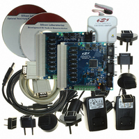
DEV KIT FOR F040/F041/F042/F043
Manufacturer
Silicon Laboratories Inc
Type
MCUr
Specifications of C8051F040DK
Contents
Evaluation Board, Power Supply, USB Cables, Adapter and Documentation
Processor To Be Evaluated
C8051F04x
Interface Type
USB
Silicon Manufacturer
Silicon Labs
Core Architecture
8051
Silicon Core Number
C8051F040
Silicon Family Name
C8051F04x
Lead Free Status / RoHS Status
Contains lead / RoHS non-compliant
For Use With/related Products
Silicon Laboratories C8051 F040, 041, 042, 043 MCUs
Lead Free Status / Rohs Status
Lead free / RoHS Compliant
Other names
336-1205
Available stocks
Company
Part Number
Manufacturer
Quantity
Price
Company:

Part Number:
C8051F040DK
Manufacturer:
SiliconL
Quantity:
9


24.2. Capture/Compare Modules
Each module can be configured to operate independently in one of six operation modes: Edge-triggered
Capture, Software Timer, High Speed Output, Frequency Output, 8-Bit Pulse Width Modulator, or 16-Bit
Pulse Width Modulator. Each module has Special Function Registers (SFRs) associated with it in the CIP-
51 system controller. These registers are used to exchange data with a module and configure the module's
mode of operation.
Table 24.2 summarizes the bit settings in the PCA0CPMn registers used to select the PCA0 capture/com-
pare module’s operating modes. Setting the ECCFn bit in a PCA0CPMn register enables the module's
CCFn interrupt. Note: PCA0 interrupts must be globally enabled before individual CCFn interrupts are rec-
ognized. PCA0 interrupts are globally enabled by setting the EA bit (IE.7) and the EPCA0 bit (EIE1.3) to
logic 1. See Figure 24.3 for details on the PCA interrupt configuration.
PWM16 ECOM CAPP CAPN MAT
X
X
X
X
X
X
0
1
Table 24.2. PCA0CPM Register Settings for PCA Capture/Compare Modules
X = Don’t Care
Timer Overflow
X
X
X
PCA Counter/
1
1
1
1
1
W
P
M
1
6
n
PCA Module 0
PCA Module 1
PCA Module 2
PCA Module 3
PCA Module 4
PCA Module 5
(for n = 0 to 5)
PCA0CPMn
C
O
M
E
n
C
A
P
P
n
CCF0
CCF1
CCF2
CCF3
CCF4
CCF5
C
A
P
N
n
M
A
T
n
1
0
1
0
0
0
0
0
O
G
T
n
W
M
P
n
E
C
C
F
n
C
Figure 24.3. PCA Interrupt Block Diagram
F
C
R
PCA0CN
C
C
F
5
0
1
1
0
0
0
0
0
C
C
F
4
C
C
F
3
C
C
F
2
C
C
F
1
C
C
F
0
ECCF0
ECCF1
ECCF2
ECCF3
ECCF4
ECCF5
0
0
0
1
1
0
0
0
C
D
L
I
PCA0MD
C
P
S
2
C
TOG PWM ECCF
P
S
1
0
1
0
1
0
1
0
1
0
1
0
1
C
P
S
0
0
0
0
0
1
1
0
0
E
C
F
0
1
Rev. 1.5
0
0
0
0
0
1
1
1
C8051F040/1/2/3/4/5/6/7
X
X
X
X
X
X
0
0
Capture triggered by transition on CEXn
Capture triggered by negative edge on
Capture triggered by positive edge on
16-Bit Pulse Width Modulator
8-Bit Pulse Width Modulator
(EIE1.3)
EPCA0
High-Speed Output
Frequency Output
Operation Mode
Software Timer
0
1
CEXn
CEXn
(IE.7)
EA
0
1
Interrupt
Priority
Decoder
305
Related parts for C8051F040DK
Image
Part Number
Description
Manufacturer
Datasheet
Request
R

Part Number:
Description:
SMD/C°/SINGLE-ENDED OUTPUT SILICON OSCILLATOR
Manufacturer:
Silicon Laboratories Inc
Part Number:
Description:
Manufacturer:
Silicon Laboratories Inc
Datasheet:
Part Number:
Description:
N/A N/A/SI4010 AES KEYFOB DEMO WITH LCD RX
Manufacturer:
Silicon Laboratories Inc
Datasheet:
Part Number:
Description:
N/A N/A/SI4010 SIMPLIFIED KEY FOB DEMO WITH LED RX
Manufacturer:
Silicon Laboratories Inc
Datasheet:
Part Number:
Description:
N/A/-40 TO 85 OC/EZLINK MODULE; F930/4432 HIGH BAND (REV E/B1)
Manufacturer:
Silicon Laboratories Inc
Part Number:
Description:
EZLink Module; F930/4432 Low Band (rev e/B1)
Manufacturer:
Silicon Laboratories Inc
Part Number:
Description:
I°/4460 10 DBM RADIO TEST CARD 434 MHZ
Manufacturer:
Silicon Laboratories Inc
Part Number:
Description:
I°/4461 14 DBM RADIO TEST CARD 868 MHZ
Manufacturer:
Silicon Laboratories Inc
Part Number:
Description:
I°/4463 20 DBM RFSWITCH RADIO TEST CARD 460 MHZ
Manufacturer:
Silicon Laboratories Inc
Part Number:
Description:
I°/4463 20 DBM RADIO TEST CARD 868 MHZ
Manufacturer:
Silicon Laboratories Inc
Part Number:
Description:
I°/4463 27 DBM RADIO TEST CARD 868 MHZ
Manufacturer:
Silicon Laboratories Inc
Part Number:
Description:
I°/4463 SKYWORKS 30 DBM RADIO TEST CARD 915 MHZ
Manufacturer:
Silicon Laboratories Inc
Part Number:
Description:
N/A N/A/-40 TO 85 OC/4463 RFMD 30 DBM RADIO TEST CARD 915 MHZ
Manufacturer:
Silicon Laboratories Inc
Part Number:
Description:
I°/4463 20 DBM RADIO TEST CARD 169 MHZ
Manufacturer:
Silicon Laboratories Inc