C8051F040DK Silicon Laboratories Inc, C8051F040DK Datasheet - Page 58
C8051F040DK
Manufacturer Part Number
C8051F040DK
Description
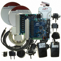
DEV KIT FOR F040/F041/F042/F043
Manufacturer
Silicon Laboratories Inc
Type
MCUr
Specifications of C8051F040DK
Contents
Evaluation Board, Power Supply, USB Cables, Adapter and Documentation
Processor To Be Evaluated
C8051F04x
Interface Type
USB
Silicon Manufacturer
Silicon Labs
Core Architecture
8051
Silicon Core Number
C8051F040
Silicon Family Name
C8051F04x
Lead Free Status / RoHS Status
Contains lead / RoHS non-compliant
For Use With/related Products
Silicon Laboratories C8051 F040, 041, 042, 043 MCUs
Lead Free Status / Rohs Status
Lead free / RoHS Compliant
Other names
336-1205
Available stocks
Company
Part Number
Manufacturer
Quantity
Price
Company:

Part Number:
C8051F040DK
Manufacturer:
SiliconL
Quantity:
9


C8051F040/1/2/3/4/5/6/7
58
Bits7-3:
Bits2-0:
AD0SC4
R/W
Bit7
AD0SC4-0: ADC0 SAR Conversion Clock Period Bits
SAR Conversion clock is derived from system clock by the following equation, where
AD0SC refers to the 5-bit value held in AD0SC4-0, and CLK
SAR clock. See Table 5.2 for SAR clock configuration requirements.
AMP0GN2-0: ADC0 Internal Amplifier Gain (PGA)
000: Gain = 1
001: Gain = 2
010: Gain = 4
011: Gain = 8
10x: Gain = 16
11x: Gain = 0.5
*Note: AD0SC is the rounded-up result.
AD0SC
AD0SC3
SFR Definition 5.5. ADC0CF: ADC0 Configuration Register
R/W
Bit6
SYSCLK
---------------------- - 1
CLK
AD0SC2
R/W
Bit5
SAR0
–
AD0SC1
R/W
Bit4
*
or
AD0SC0 AMP0GN2 AMP0GN1 AMP0GN0 11111000
Rev. 1.5
R/W
Bit3
CLK
SAR0
R/W
Bit2
=
----------------------------
AD0SC
SYSCLK
SAR0
R/W
Bit1
refers to the desired ADC0
+
1
SFR Address:
SFR Page:
R/W
Bit0
0xBC
0
Reset Value
Related parts for C8051F040DK
Image
Part Number
Description
Manufacturer
Datasheet
Request
R

Part Number:
Description:
SMD/C°/SINGLE-ENDED OUTPUT SILICON OSCILLATOR
Manufacturer:
Silicon Laboratories Inc
Part Number:
Description:
Manufacturer:
Silicon Laboratories Inc
Datasheet:
Part Number:
Description:
N/A N/A/SI4010 AES KEYFOB DEMO WITH LCD RX
Manufacturer:
Silicon Laboratories Inc
Datasheet:
Part Number:
Description:
N/A N/A/SI4010 SIMPLIFIED KEY FOB DEMO WITH LED RX
Manufacturer:
Silicon Laboratories Inc
Datasheet:
Part Number:
Description:
N/A/-40 TO 85 OC/EZLINK MODULE; F930/4432 HIGH BAND (REV E/B1)
Manufacturer:
Silicon Laboratories Inc
Part Number:
Description:
EZLink Module; F930/4432 Low Band (rev e/B1)
Manufacturer:
Silicon Laboratories Inc
Part Number:
Description:
I°/4460 10 DBM RADIO TEST CARD 434 MHZ
Manufacturer:
Silicon Laboratories Inc
Part Number:
Description:
I°/4461 14 DBM RADIO TEST CARD 868 MHZ
Manufacturer:
Silicon Laboratories Inc
Part Number:
Description:
I°/4463 20 DBM RFSWITCH RADIO TEST CARD 460 MHZ
Manufacturer:
Silicon Laboratories Inc
Part Number:
Description:
I°/4463 20 DBM RADIO TEST CARD 868 MHZ
Manufacturer:
Silicon Laboratories Inc
Part Number:
Description:
I°/4463 27 DBM RADIO TEST CARD 868 MHZ
Manufacturer:
Silicon Laboratories Inc
Part Number:
Description:
I°/4463 SKYWORKS 30 DBM RADIO TEST CARD 915 MHZ
Manufacturer:
Silicon Laboratories Inc
Part Number:
Description:
N/A N/A/-40 TO 85 OC/4463 RFMD 30 DBM RADIO TEST CARD 915 MHZ
Manufacturer:
Silicon Laboratories Inc
Part Number:
Description:
I°/4463 20 DBM RADIO TEST CARD 169 MHZ
Manufacturer:
Silicon Laboratories Inc