MAX3420EEVKIT-2+ Maxim Integrated Products, MAX3420EEVKIT-2+ Datasheet - Page 8
MAX3420EEVKIT-2+
Manufacturer Part Number
MAX3420EEVKIT-2+
Description
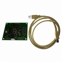
EVAL KIT FOR MAX3420E
Manufacturer
Maxim Integrated Products
Specifications of MAX3420EEVKIT-2+
Main Purpose
Interface, USB 2.0 Slave
Embedded
No
Utilized Ic / Part
MAX3420E
Primary Attributes
Full Speed (12Mbps), SPI Interface, No Custom USB Drivers
Secondary Attributes
4 GPI Pushbuttons, 4 GPO LEDs
Lead Free Status / RoHS Status
Lead free / RoHS Compliant


ABSOLUTE MAXIMUM RATINGS
(All voltages referenced to GND, unless otherwise noted.)
V
V
VBCOMP .................................................................-0.3V to +6V
D+, D-, XI, XO ............................................-0.3V to (V
SCLK, MOSI, MISO, SS, RES, GPOUT3–GPOUT0,
USB Peripheral Controller
with SPI Interface
Stresses beyond those listed under “Absolute Maximum Ratings” may cause permanent damage to the device. These are stress ratings only, and functional
operation of the device at these or any other conditions beyond those indicated in the operational sections of the specifications is not implied. Exposure to
absolute maximum rating conditions for extended periods may affect device reliability.
ELECTRICAL CHARACTERISTICS
(V
+2.5V, T
8
DC CHARACTERISTICS
Supply Voltage V
Logic-Core Supply and Logic-
Interface Voltage V
V
V
V
V
V
LOGIC-SIDE I/O
MISO, GPOUT3–GPOUT0, GPX,
INT Output High Voltage
MISO, GPOUT3–GPOUT0, GPX,
INT Output Low Voltage
SCLK, MOSI, GPIN3–GPIN0, SS,
RES Input High Voltage
SCLK, MOSI, GPIN3–GPIN0, SS,
RES Input Low Voltage
SCLK, MOSI, SS, RES Input
Leakage Current
GP IN 3–GP IN 0 P ul l up Resi stor to V
TRANSCEIVER SPECIFICATIONS
Differential-Receiver Input
Sensitivity
Differential-Receiver Common-
Mode Voltage
CC
L
CC
GPIN3–GPIN0, GPX, INT ..........................-0.3V to (V
CC
L
CC
CC
L
.............................................................................-0.3V to +4V
S usp end S up p l y C urr ent
Supply Current
_______________________________________________________________________________________
......................................................................... -0.3V to +4V
Supply Current
Supply Current During Idle
Suspend Supply Current
= +3V to +3.6V, V
A
= +25°C.) (Note 1)
PARAMETER
CC
L
L
= +1.71V to +3.6V, T
L
SYMBOL
I
R
CCSUS
I
I
V
LSUS
V
CCID
V
I
V
V
GPIN
V
CC
I
I
OH
CC
OL
IL
L
IH
IL
L
A
Continuously transmitting on D+ and D- at
12Mbps, C
CONNECT = 0
SCLK toggling at 20MHz, SS = low,
GPIN3–GPIN0 = 0
D+ = high, D- = low
CONNECT = 0, PWRDOWN = 1
CONNECT = 0, PWRDOWN = 1
I
I
I
I
|V
= T
LOAD
LOAD
LOAD
LOAD
D+
CC
MIN
L
- V
+ 0.3V)
+ 0.3V)
= +5mA, V
= +10mA, V
= -20mA, V
= -20mA, V
D-
to T
|
L
MAX
= 50pF on D+ and D- to GND,
CONDITIONS
, unless otherwise noted. Typical values are at V
L
L
L
L
< 2.5V
< 2.5V
≥ 2.5V
Continuous Power Dissipation (T
Operating Temperature Range ...........................-40°C to +85°C
Junction Temperature ......................................................+150°C
Storage Temperature Range .............................-65°C to +150°C
Lead Temperature (soldering, 10s) .................................+300°C
Soldering Temperature (reflow) .......................................+260°C
≥ 2.5V
24-Pin TQFN (derate 20.8mW/°C above +70°C) .......1667mW
32-Pin LQFP (derate 20.7mW/°C above +70°C)........1653mW
V
2/3 x V
V
L
1.71
L
MIN
3.0
0.2
0.8
- 0.45
10
- 0.4
A
L
= +70°C)
TYP
3.3
1.5
15
33
15
20
6
CC
MAX
3.60
100
3.6
0.6
0.4
0.4
2.5
30
20
50
30
5
1
= +3.3V, V
UNITS
mA
mA
mA
kΩ
µA
µA
µA
V
V
V
V
V
V
V
V
L
=
Related parts for MAX3420EEVKIT-2+
Image
Part Number
Description
Manufacturer
Datasheet
Request
R

Part Number:
Description:
MAX7528KCWPMaxim Integrated Products [CMOS Dual 8-Bit Buffered Multiplying DACs]
Manufacturer:
Maxim Integrated Products
Datasheet:
Part Number:
Description:
Single +5V, fully integrated, 1.25Gbps laser diode driver.
Manufacturer:
Maxim Integrated Products
Datasheet:
Part Number:
Description:
Single +5V, fully integrated, 155Mbps laser diode driver.
Manufacturer:
Maxim Integrated Products
Datasheet:
Part Number:
Description:
VRD11/VRD10, K8 Rev F 2/3/4-Phase PWM Controllers with Integrated Dual MOSFET Drivers
Manufacturer:
Maxim Integrated Products
Datasheet:
Part Number:
Description:
Highly Integrated Level 2 SMBus Battery Chargers
Manufacturer:
Maxim Integrated Products
Datasheet:
Part Number:
Description:
Current Monitor and Accumulator with Integrated Sense Resistor; ; Temperature Range: -40°C to +85°C
Manufacturer:
Maxim Integrated Products
Part Number:
Description:
TSSOP 14/A�/RS-485 Transceivers with Integrated 100O/120O Termination Resis
Manufacturer:
Maxim Integrated Products
Part Number:
Description:
TSSOP 14/A�/RS-485 Transceivers with Integrated 100O/120O Termination Resis
Manufacturer:
Maxim Integrated Products
Part Number:
Description:
QFN 16/A�/AC-DC and DC-DC Peak-Current-Mode Converters with Integrated Step
Manufacturer:
Maxim Integrated Products
Part Number:
Description:
TDFN/A/65V, 1A, 600KHZ, SYNCHRONOUS STEP-DOWN REGULATOR WITH INTEGRATED SWI
Manufacturer:
Maxim Integrated Products
Part Number:
Description:
Integrated Temperature Controller f
Manufacturer:
Maxim Integrated Products
Part Number:
Description:
SOT23-6/I�/45MHz to 650MHz, Integrated IF VCOs with Differential Output
Manufacturer:
Maxim Integrated Products
Part Number:
Description:
SOT23-6/I�/45MHz to 650MHz, Integrated IF VCOs with Differential Output
Manufacturer:
Maxim Integrated Products
Part Number:
Description:
EVALUATION KIT/2.4GHZ TO 2.5GHZ 802.11G/B RF TRANSCEIVER WITH INTEGRATED PA
Manufacturer:
Maxim Integrated Products
Part Number:
Description:
QFN/E/DUAL PCIE/SATA HIGH SPEED SWITCH WITH INTEGRATED BIAS RESISTOR
Manufacturer:
Maxim Integrated Products
Datasheet: