MAX3420EEVKIT-2+ Maxim Integrated Products, MAX3420EEVKIT-2+ Datasheet - Page 14
MAX3420EEVKIT-2+
Manufacturer Part Number
MAX3420EEVKIT-2+
Description
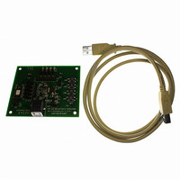
EVAL KIT FOR MAX3420E
Manufacturer
Maxim Integrated Products
Specifications of MAX3420EEVKIT-2+
Main Purpose
Interface, USB 2.0 Slave
Embedded
No
Utilized Ic / Part
MAX3420E
Primary Attributes
Full Speed (12Mbps), SPI Interface, No Custom USB Drivers
Secondary Attributes
4 GPI Pushbuttons, 4 GPO LEDs
Lead Free Status / RoHS Status
Lead free / RoHS Compliant


pending (Figure 10). Set the POSINT bit in the PINCTL
(R17) register to make INT active high, and clear the
POSINT bit to make INT active low.
The MAX3420E has four general-purpose inputs
(GPIN3–GPIN0), four general-purpose outputs
(GPOUT3–GPOUT0), and a multiplexed output pin
(GPX). GPIN3 through GPIN0 all have weak internal
pullup resistors to V
sampling bits 7 through 4 of the IOPINS (R20) register.
Writing to GPIN3 through GPIN0 has no effect.
GPOUT3 through GPOUT0 are the general-purpose
outputs. Update these outputs by writing to bits 3
through 0 of the IOPINS (R20) register. GPOUT3–
GPOUT0 logic levels are referenced to the voltage on
V
GPOUT3–GPOUT0 bit returns the state of the internal
register bit, not the actual pin state. This is useful for
doing read-modify-write operations to an output pin
(such as blinking an LED), since the load on the output
pin does not affect the register logic state.
GPX is a push-pull output with a 4-way multiplexer that
selects its output signal. The logic level on GPX is refer-
enced to V
GPXA bits of PINCTL (R17) register to select one of four
internal signals as depicted in Table 3.
USB Peripheral Controller
with SPI Interface
Table 3. GPX Output State
14
14
L
GPIN3–GPIN0, GPOUT3–GPOUT0 and GPX
. As shown in Figure 11, reading the state of a
• OPERATE: This signal goes high when the
• VBUS_DET: VBUS_DET is the VBCOMP comparator
• BUSACT: USB BUS activity signal (active-high).
• SOF: A square wave with a positive edge that
GPXB
MAX3420E is able to operate after a power-up or
RES reset. OPERATE is the default GPX output.
output. This allows the user to directly monitor the
V
This signal is active whenever there is traffic on
the USB bus. The BUSACT signal is set whenever
a SYNC field is detected. BUSACT goes low during
bus reset or after 32-bit times of J-state.
indicates the USB start-of-frame (Figure 12).
______________________________________________________________________________________
______________________________________________________________________________________
0
0
1
1
BUS
status.
L
. The SPI master writes to the GPXB and
GPXA
0
1
0
1
L
. These inputs can be read by
GPX PIN OUTPUT
OPERATE (Default State)
VBUS_DET
BUSACT
SOF
The SPI data pins MOSI and MISO operate differently
depending on the setting of a register bit called FDUPSPI
(full-duplex SPI). Figure 13 shows the two configurations
according to the FDUPSPI bit setting.
Figure 11. Behavior of Read and Write Operations on
GPOUT3–GPOUT0
Figure 12. GPX Output in SOF Mode
Figure 13. MAX3420E SPI Data Pins for Full-Duplex (Top) and
Half-Duplex (Bottom) Operation
PACKETS
GPOUT
GPOUT
WRITE
READ
USB
GPX
SOF
FDUPSPI = 1
FDUPSPI = 0
~50%
(DEFAULT)
FULL-SPEED
TIME FRAME
REGISTER BIT
MOSI (Master-Out, Slave-In) and
1ms
MISO (Master-In, Slave-Out)
SOF
MAX3420E
MAX3420E
FULL-SPEED
TIME FRAME
1ms
MOSI
MISO
MOSI
MISO
GPOUT
SOF
PIN
Related parts for MAX3420EEVKIT-2+
Image
Part Number
Description
Manufacturer
Datasheet
Request
R

Part Number:
Description:
MAX7528KCWPMaxim Integrated Products [CMOS Dual 8-Bit Buffered Multiplying DACs]
Manufacturer:
Maxim Integrated Products
Datasheet:
Part Number:
Description:
Single +5V, fully integrated, 1.25Gbps laser diode driver.
Manufacturer:
Maxim Integrated Products
Datasheet:
Part Number:
Description:
Single +5V, fully integrated, 155Mbps laser diode driver.
Manufacturer:
Maxim Integrated Products
Datasheet:
Part Number:
Description:
VRD11/VRD10, K8 Rev F 2/3/4-Phase PWM Controllers with Integrated Dual MOSFET Drivers
Manufacturer:
Maxim Integrated Products
Datasheet:
Part Number:
Description:
Highly Integrated Level 2 SMBus Battery Chargers
Manufacturer:
Maxim Integrated Products
Datasheet:
Part Number:
Description:
Current Monitor and Accumulator with Integrated Sense Resistor; ; Temperature Range: -40°C to +85°C
Manufacturer:
Maxim Integrated Products
Part Number:
Description:
TSSOP 14/A�/RS-485 Transceivers with Integrated 100O/120O Termination Resis
Manufacturer:
Maxim Integrated Products
Part Number:
Description:
TSSOP 14/A�/RS-485 Transceivers with Integrated 100O/120O Termination Resis
Manufacturer:
Maxim Integrated Products
Part Number:
Description:
QFN 16/A�/AC-DC and DC-DC Peak-Current-Mode Converters with Integrated Step
Manufacturer:
Maxim Integrated Products
Part Number:
Description:
TDFN/A/65V, 1A, 600KHZ, SYNCHRONOUS STEP-DOWN REGULATOR WITH INTEGRATED SWI
Manufacturer:
Maxim Integrated Products
Part Number:
Description:
Integrated Temperature Controller f
Manufacturer:
Maxim Integrated Products
Part Number:
Description:
SOT23-6/I�/45MHz to 650MHz, Integrated IF VCOs with Differential Output
Manufacturer:
Maxim Integrated Products
Part Number:
Description:
SOT23-6/I�/45MHz to 650MHz, Integrated IF VCOs with Differential Output
Manufacturer:
Maxim Integrated Products
Part Number:
Description:
EVALUATION KIT/2.4GHZ TO 2.5GHZ 802.11G/B RF TRANSCEIVER WITH INTEGRATED PA
Manufacturer:
Maxim Integrated Products
Part Number:
Description:
QFN/E/DUAL PCIE/SATA HIGH SPEED SWITCH WITH INTEGRATED BIAS RESISTOR
Manufacturer:
Maxim Integrated Products
Datasheet: