MAX3420EEVKIT-2+ Maxim Integrated Products, MAX3420EEVKIT-2+ Datasheet - Page 16
MAX3420EEVKIT-2+
Manufacturer Part Number
MAX3420EEVKIT-2+
Description
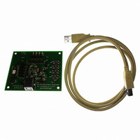
EVAL KIT FOR MAX3420E
Manufacturer
Maxim Integrated Products
Specifications of MAX3420EEVKIT-2+
Main Purpose
Interface, USB 2.0 Slave
Embedded
No
Utilized Ic / Part
MAX3420E
Primary Attributes
Full Speed (12Mbps), SPI Interface, No Custom USB Drivers
Secondary Attributes
4 GPI Pushbuttons, 4 GPO LEDs
Lead Free Status / RoHS Status
Lead free / RoHS Compliant


The MAX3420E can be programmed to operate in half-
duplex (a bidirectional data pin) or full-duplex (one
data-in and one data-out pin) mode. The SPI master
sets a register bit called FDUPSPI (full-duplex SPI) to 1
for full-duplex, and 0 for half-duplex operation. Half-
duplex is the power-on default.
When the SPI master sets FDUPSPI = 1, the SPI inter-
face uses separate data pins, MOSI and MISO to trans-
fer data. Because of the separate data pins, bits can
be simultaneously clocked into and out of the
MAX3420E. The MAX3420E makes use of this feature
by clocking out 8 USB status bits as the command byte
is clocked in, as illustrated in Figure 15.
In full-duplex mode the SPI master reads data from the
MAX3420E slave interface using the following steps:
(1) When SS is high, the MAX3420E is unselected and
(2) After driving SCLK to its inactive state, the SPI master
(3) The SPI master simultaneously clocks the com-
(4) After eight clock cycles, the master can drive SS
(5) By keeping SS low, the master clocks register data
In full-duplex mode, the SPI master writes data to the
MAX3420E slave interface through the following steps:
USB Peripheral Controller
with SPI Interface
16
tri-states the MISO output.
selects the MAX3420E by driving SS low. The
MAX3420E turns on its MISO output buffer and places
the first data bit (Q7) on the MISO output (Figure 14).
mand byte into the MAX3420E MOSI pin, and USB
status bits out of the MAX3420E MISO pin on the
rising edges of the SCLK it supplies. The
MAX3420E changes its MISO output data on the
falling edges of SCLK.
high to deselect the MAX3420E, causing it to tri-
state its MISO output. The falling edge of the clock
puts the MSB of the next data byte in the sequence
on the MISO output (Figure 14).
bytes out of the MAX3420E by continuing to supply
SCLK pulses (burst mode). The master terminates
the transfer by driving SS high. The master must
ensure that SCLK is in its inactive state at the
beginning of the next access (when it drives SS
low). In full-duplex mode, the MAX3420E ignores
data on MOSI while clocking data out on MISO.
______________________________________________________________________________________
Reading from the SPI Slave Interface (MISO)
SPI Half- and Full-Duplex Operation
Writing to the SPI Slave Interface (MOSI)
Full-Duplex Operation
in Full-Duplex Mode
in Full-Duplex Mode
(1) The SPI master sets the clock to its inactive state.
(2) The SPI master selects the MAX3420E by driving
(3) The SPI master simultaneously clocks the com-
(4) After eight clock cycles, the master can drive SS
(5) By keeping SS low, the master clocks data bytes
The MAX3420E is put into half-duplex mode at power-
on, or when the SPI master clears the FDUPSPI bit. In
half-duplex mode, the MAX3420E tri-states its MISO pin
and makes the MOSI pin bidirectional, saving a pin in
the SPI interface. The MISO pin can be left unconnect-
ed in half-duplex operation.
Because of the single data pin, the USB status bits
available in full-duplex mode are not available as the
SPI master clocks in the command byte. In half-duplex
mode these status bits are accessed in the normal way,
as register bits.
The SPI master must operate the MOSI pin as bidirec-
tional. It accesses a MAX3420E register as follows:
(1) The SPI master sets the clock to its inactive state.
(2) The SPI master selects the MAX3420E by driving
(3) The SPI master turns on its output driver and clocks
(4) After eight clock cycles, the master can drive SS
While SS is high, the master can drive the MOSI pin.
SS low and placing the first data bit to write on the
MOSI input.
mand byte into the MAX3420E and USB status bits
out of the MAX3420E MISO pin on the rising edges
of the SCLK it supplies. The SPI master changes its
MOSI input data on the falling edges of SCLK.
high to deselect the MAX3420E.
into the MAX3420E by continuing to supply SCLK
pulses (burst mode). The master terminates the
transfer by driving SS high. The master must ensure
that SCLK is inactive at the beginning of the next
access (when it drives SS low). In full-duplex mode,
the MAX3420E outputs USB status bits on MISO
during the first 8 bits (the command byte), and sub-
sequently outputs zeroes on MISO as the SPI mas-
ter clocks bytes into MOSI.
While SS is high, the master can drive the MOSI pin
to any value.
SS low and placing the first data bit (MSB) to write
on the MOSI input.
the command byte into the MAX3420E on the rising
edges of the SCLK it supplies. The SPI master
changes its MOSI data on the falling edges of SCLK.
high to deselect the MAX3420E.
Half-Duplex Operation
Related parts for MAX3420EEVKIT-2+
Image
Part Number
Description
Manufacturer
Datasheet
Request
R

Part Number:
Description:
MAX7528KCWPMaxim Integrated Products [CMOS Dual 8-Bit Buffered Multiplying DACs]
Manufacturer:
Maxim Integrated Products
Datasheet:
Part Number:
Description:
Single +5V, fully integrated, 1.25Gbps laser diode driver.
Manufacturer:
Maxim Integrated Products
Datasheet:
Part Number:
Description:
Single +5V, fully integrated, 155Mbps laser diode driver.
Manufacturer:
Maxim Integrated Products
Datasheet:
Part Number:
Description:
VRD11/VRD10, K8 Rev F 2/3/4-Phase PWM Controllers with Integrated Dual MOSFET Drivers
Manufacturer:
Maxim Integrated Products
Datasheet:
Part Number:
Description:
Highly Integrated Level 2 SMBus Battery Chargers
Manufacturer:
Maxim Integrated Products
Datasheet:
Part Number:
Description:
Current Monitor and Accumulator with Integrated Sense Resistor; ; Temperature Range: -40°C to +85°C
Manufacturer:
Maxim Integrated Products
Part Number:
Description:
TSSOP 14/A�/RS-485 Transceivers with Integrated 100O/120O Termination Resis
Manufacturer:
Maxim Integrated Products
Part Number:
Description:
TSSOP 14/A�/RS-485 Transceivers with Integrated 100O/120O Termination Resis
Manufacturer:
Maxim Integrated Products
Part Number:
Description:
QFN 16/A�/AC-DC and DC-DC Peak-Current-Mode Converters with Integrated Step
Manufacturer:
Maxim Integrated Products
Part Number:
Description:
TDFN/A/65V, 1A, 600KHZ, SYNCHRONOUS STEP-DOWN REGULATOR WITH INTEGRATED SWI
Manufacturer:
Maxim Integrated Products
Part Number:
Description:
Integrated Temperature Controller f
Manufacturer:
Maxim Integrated Products
Part Number:
Description:
SOT23-6/I�/45MHz to 650MHz, Integrated IF VCOs with Differential Output
Manufacturer:
Maxim Integrated Products
Part Number:
Description:
SOT23-6/I�/45MHz to 650MHz, Integrated IF VCOs with Differential Output
Manufacturer:
Maxim Integrated Products
Part Number:
Description:
EVALUATION KIT/2.4GHZ TO 2.5GHZ 802.11G/B RF TRANSCEIVER WITH INTEGRATED PA
Manufacturer:
Maxim Integrated Products
Part Number:
Description:
QFN/E/DUAL PCIE/SATA HIGH SPEED SWITCH WITH INTEGRATED BIAS RESISTOR
Manufacturer:
Maxim Integrated Products
Datasheet: