MAX3420EEVKIT-2+ Maxim Integrated Products, MAX3420EEVKIT-2+ Datasheet - Page 13
MAX3420EEVKIT-2+
Manufacturer Part Number
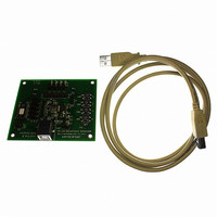
MAX3420EEVKIT-2+
Description
EVAL KIT FOR MAX3420E
Manufacturer
Maxim Integrated Products
Specifications of MAX3420EEVKIT-2+
Main Purpose
Interface, USB 2.0 Slave
Embedded
No
Utilized Ic / Part
MAX3420E
Primary Attributes
Full Speed (12Mbps), SPI Interface, No Custom USB Drivers
Secondary Attributes
4 GPI Pushbuttons, 4 GPO LEDs
Lead Free Status / RoHS Status
Lead free / RoHS Compliant


Table 2. Internal Pullup Resistor Control
(NOVBUSIRQ)) and disconnect the internal 1.5kΩ
pullup resistor. If the device using the MAX3420E is
bus powered (through a +3.3V regulator connected to
V
general-purpose input. Using VBCOMP as a general-
purpose input requires a 10kΩ pullup resistor from
VBCOMP to V
tion for more details about this connection.
The internal USB full-speed transceiver is brought out
to the bidirectional data pins D+ and D-. These pins are
±15kV ESD protected. Connect D+ and D- to a USB
“B” connector through 33Ω ±1% series resistors. A
switchable 1.5kΩ pullup resistor is internally connected
to D+. According to the USB rev 2.0 specification, a
self-powered peripheral must disconnect its 1.5kΩ
pullup resistor to D+ in the event that the host turns off
bus power. The VBGATE bit in the USBCTL (R15) regis-
ter provides the option for the MAX3420E internal logic
to automatically disconnect the 1.5kΩ resistor on D+.
The VBGATE and CONNECT bits of USBCTL (R15),
along with the VBCOMP comparator output
(VBUS_DET), control the pullup resistor between V
and D+, as shown in Table 2. Note that if VBGATE = 1
and VBUS_DET = 0, the pullup resistor is disconnected
regardless of the CONNECT bit setting.
XI and XO connect an external 12MHz crystal to the
internal oscillator circuit. XI is the crystal oscillator
input, and XO is the crystal oscillator output. Connect
one side of an external 12MHz ±0.25% parallel reso-
nant crystal to XI, and connect XO to the other side.
Connect load capacitors (20pF max) to ground on both
XI and XO. XI can also be driven with an external
12MHz ±0.25% clock. If driving XI with an external
clock, leave XO unconnected. The external clock must
meet the voltage characteristics depicted in the
Electrical Characteristics table. Internal logic is single-
edge triggered. The external clock should have a nomi-
nal 50% duty cycle.
CONNECT
CC
), the MAX3420E VBCOMP input can be used as a
0
1
1
1
VBGATE
L
. See the Applications Information sec-
X
0
1
1
______________________________________________________________________________________
VBUS_DET
X
X
0
1
Not Connected
Not Connected
Connected
Connected
XI and XO
PULLUP
D+ and D-
CC
USB Peripheral Controller
Drive RES low to put the MAX3420E into a chip reset. A
chip reset sets all registers to their default states,
except for PINCTL (R17), USBCTL (R15), and SPI logic.
All FIFO contents are unknown during chip reset. Bring
the MAX3420E out of chip reset by driving RES high.
The RES pulse width can be as short as 200ns. See the
Device Reset section for a description of the resets
available on the MAX3420E.
The MAX3420E INT output pin signals when a USB
event occurs that requires the attention of the SPI mas-
ter. The SPI master must set the IE bit in the CPUCTL
(R16) register to activate INT. When the IE bit is
cleared, INT is inactive (open for level mode, high for
negative edge, low for positive edge). INT is inactive
upon power-up or after a chip reset.
The INT pin can be a push-pull or open-drain output.
Set the INTLEVEL bit of the PINCTL (R17) register high
to program the INT output pin to be an active-low level
(open-drain output). An external pullup resistor to V
required for this setting. In level mode, the MAX3420E
drives INT low when any of the interrupt flags are set. If
multiple interrupts are pending, INT goes inactive only
when the SPI master clears the last active interrupt
request bit (Figure 10). The POSINT bit of the PINCTL
(R17) register has no effect on INT in level mode.
Clear the INTLEVEL bit to program INT to be an edge
(push-pull output). The active edge is programmable
using the POSINT bit of the PINCTL (R17) register. In
edge mode, the MAX3420E produces an edge refer-
enced to V
or when an interrupt request is cleared and others are
Figure 10. Behavior of the INT Pin for Different INTLEVEL and
POSINT Bit Settings
(1) WIDTH DETERMINED BY TIME TAKEN TO CLEAR THE IRQ
(2) 10.67μs
INTLEVEL = 1
INTLEVEL = 0
INTLEVEL = 0
POSINT = X
POSINT = 0
POSINT = 1
SINGLE
IRQ
L
with SPI Interface
(1)
any time an interrupt request is activated,
CLEAR
IRQ
FIRST IRQ
ACTIVE
(2)
SECOND
ACTIVE
IRQ
FIRST IRQ,
IRQ STILL
SECOND
ACTIVE
CLEAR
,
PENDING
CLEAR
LAST
IRQ
RES
INT
INT
INT
INT
L
13
is
Related parts for MAX3420EEVKIT-2+
Image
Part Number
Description
Manufacturer
Datasheet
Request
R

Part Number:
Description:
MAX7528KCWPMaxim Integrated Products [CMOS Dual 8-Bit Buffered Multiplying DACs]
Manufacturer:
Maxim Integrated Products
Datasheet:
Part Number:
Description:
Single +5V, fully integrated, 1.25Gbps laser diode driver.
Manufacturer:
Maxim Integrated Products
Datasheet:
Part Number:
Description:
Single +5V, fully integrated, 155Mbps laser diode driver.
Manufacturer:
Maxim Integrated Products
Datasheet:
Part Number:
Description:
VRD11/VRD10, K8 Rev F 2/3/4-Phase PWM Controllers with Integrated Dual MOSFET Drivers
Manufacturer:
Maxim Integrated Products
Datasheet:
Part Number:
Description:
Highly Integrated Level 2 SMBus Battery Chargers
Manufacturer:
Maxim Integrated Products
Datasheet:
Part Number:
Description:
Current Monitor and Accumulator with Integrated Sense Resistor; ; Temperature Range: -40°C to +85°C
Manufacturer:
Maxim Integrated Products
Part Number:
Description:
TSSOP 14/A�/RS-485 Transceivers with Integrated 100O/120O Termination Resis
Manufacturer:
Maxim Integrated Products
Part Number:
Description:
TSSOP 14/A�/RS-485 Transceivers with Integrated 100O/120O Termination Resis
Manufacturer:
Maxim Integrated Products
Part Number:
Description:
QFN 16/A�/AC-DC and DC-DC Peak-Current-Mode Converters with Integrated Step
Manufacturer:
Maxim Integrated Products
Part Number:
Description:
TDFN/A/65V, 1A, 600KHZ, SYNCHRONOUS STEP-DOWN REGULATOR WITH INTEGRATED SWI
Manufacturer:
Maxim Integrated Products
Part Number:
Description:
Integrated Temperature Controller f
Manufacturer:
Maxim Integrated Products
Part Number:
Description:
SOT23-6/I�/45MHz to 650MHz, Integrated IF VCOs with Differential Output
Manufacturer:
Maxim Integrated Products
Part Number:
Description:
SOT23-6/I�/45MHz to 650MHz, Integrated IF VCOs with Differential Output
Manufacturer:
Maxim Integrated Products
Part Number:
Description:
EVALUATION KIT/2.4GHZ TO 2.5GHZ 802.11G/B RF TRANSCEIVER WITH INTEGRATED PA
Manufacturer:
Maxim Integrated Products
Part Number:
Description:
QFN/E/DUAL PCIE/SATA HIGH SPEED SWITCH WITH INTEGRATED BIAS RESISTOR
Manufacturer:
Maxim Integrated Products
Datasheet: