MAX3420EEVKIT-2+ Maxim Integrated Products, MAX3420EEVKIT-2+ Datasheet - Page 15
MAX3420EEVKIT-2+
Manufacturer Part Number
MAX3420EEVKIT-2+
Description
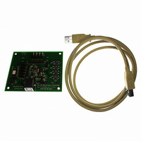
EVAL KIT FOR MAX3420E
Manufacturer
Maxim Integrated Products
Specifications of MAX3420EEVKIT-2+
Main Purpose
Interface, USB 2.0 Slave
Embedded
No
Utilized Ic / Part
MAX3420E
Primary Attributes
Full Speed (12Mbps), SPI Interface, No Custom USB Drivers
Secondary Attributes
4 GPI Pushbuttons, 4 GPO LEDs
Lead Free Status / RoHS Status
Lead free / RoHS Compliant


Figure 14. SPI Clocking Modes
In full-duplex mode (FDUPSPI = 1), the MOSI and MISO
pins are separate, and the MISO pin drives only when SS
is low. In this mode, the first eight SCLK edges (after SS =
0) clock the command byte into the MAX3420E on MOSI,
and eight USB status bits are clocked out of the
MAX3420E on MISO. For an SPI write cycle, any bytes
following the command byte are clocked into the
MAX3420E on MOSI, and zeros are clocked out on MISO.
For an SPI read cycle, any bytes following the command
byte are clocked out of the MAX3420E on MISO and the
data on MOSI is ignored. At the conclusion of the SPI
cycle (SS = 1), the MISO output tri-states.
In half-duplex mode, the MOSI pin is a bidirectional pin
and the MISO pin is tri-stated. This saves a pin in the SPI
interface. Because of the shared data pin, this mode
does not offer the eight USB status bits (Figure 5) as the
command byte is clocked into the MAX3420E. The MISO
pin can be left unconnected in half-duplex mode.
The SPI master provides the MAX3420E SCLK signal to
clock the SPI interface. SCLK has no low-frequency limit,
and can be as high as 26MHz. The MAX3420E changes
its output data (MISO) on the falling edge of SCLK and
samples input data (MOSI) on the rising edge of SCLK.
The MAX3420E ignores SCLK transitions when SS is
high. The inactive level of SCLK may be low or high,
depending on the SPI operating mode (Figure 14).
The MAX3420E SPI interface is active only when SS is
low. When SS is high, the MAX3420E tri-states the SPI
output pin and resets the internal MAX3420E SPI logic.
MODE 0,0
MODE 1,1
MISO
SCLK
SCLK
MOSI
SS
______________________________________________________________________________________
D7
Q7
SCLK (Serial Clock)
SS (Slave Select)
D6
Q6
D5
Q5
*MSB OF NEXT BYTE IN BURST MODE (SS REMAINS LOW)
D4
USB Peripheral Controller
Q4
SPI MODE 0,0 OR 1,1
If SS goes high before a complete byte is clocked in,
the byte-in-progress is discarded. The SPI master can
terminate an SPI cycle after clocking in the first 8 bits
(the command byte). This feature can be used in a full-
duplex system to retrieve the USB status bits (Figure 5)
without sending or receiving SPI data.
The MAX3420E operates as an SPI slave device. A reg-
ister access consists of the SPI master first writing an
SPI command byte, followed by reading or writing the
contents of the addressed register (see the Register
Description section for more details). All SPI transfers
are MSB first. The external SPI master provides a clock
signal to the MAX3420E SCLK input. This clock fre-
quency can be between DC and 26MHz. Bit transfers
occur on the positive edge of SCLK. The MAX3420E
counts bits and divides them into bytes. If fewer than 8
bits are clocked into the MAX3420E when SS goes
high, the MAX3420E discards the partial byte.
The MAX3420E SPI interface operates without adjust-
ment in either SPI mode (CPOL = 0, CPHA = 0) or
(CPOL = 1, CPHA = 1). No mode bit is required to
select between the two modes since the interface uses
the rising edge of the clock in both modes. The two
clocking modes are illustrated in Figure 14. Note that
the inactive SCLK value is different for the two modes.
Figure 14 illustrates the full-duplex mode, where data is
simultaneously clocked into and out of the MAX3420E.
D3
Q3
D2
with SPI Interface
Q2
Applications Information
D1
Q1
D0
Q0
*
SPI Interface
*
15
Related parts for MAX3420EEVKIT-2+
Image
Part Number
Description
Manufacturer
Datasheet
Request
R

Part Number:
Description:
MAX7528KCWPMaxim Integrated Products [CMOS Dual 8-Bit Buffered Multiplying DACs]
Manufacturer:
Maxim Integrated Products
Datasheet:
Part Number:
Description:
Single +5V, fully integrated, 1.25Gbps laser diode driver.
Manufacturer:
Maxim Integrated Products
Datasheet:
Part Number:
Description:
Single +5V, fully integrated, 155Mbps laser diode driver.
Manufacturer:
Maxim Integrated Products
Datasheet:
Part Number:
Description:
VRD11/VRD10, K8 Rev F 2/3/4-Phase PWM Controllers with Integrated Dual MOSFET Drivers
Manufacturer:
Maxim Integrated Products
Datasheet:
Part Number:
Description:
Highly Integrated Level 2 SMBus Battery Chargers
Manufacturer:
Maxim Integrated Products
Datasheet:
Part Number:
Description:
Current Monitor and Accumulator with Integrated Sense Resistor; ; Temperature Range: -40°C to +85°C
Manufacturer:
Maxim Integrated Products
Part Number:
Description:
TSSOP 14/A�/RS-485 Transceivers with Integrated 100O/120O Termination Resis
Manufacturer:
Maxim Integrated Products
Part Number:
Description:
TSSOP 14/A�/RS-485 Transceivers with Integrated 100O/120O Termination Resis
Manufacturer:
Maxim Integrated Products
Part Number:
Description:
QFN 16/A�/AC-DC and DC-DC Peak-Current-Mode Converters with Integrated Step
Manufacturer:
Maxim Integrated Products
Part Number:
Description:
TDFN/A/65V, 1A, 600KHZ, SYNCHRONOUS STEP-DOWN REGULATOR WITH INTEGRATED SWI
Manufacturer:
Maxim Integrated Products
Part Number:
Description:
Integrated Temperature Controller f
Manufacturer:
Maxim Integrated Products
Part Number:
Description:
SOT23-6/I�/45MHz to 650MHz, Integrated IF VCOs with Differential Output
Manufacturer:
Maxim Integrated Products
Part Number:
Description:
SOT23-6/I�/45MHz to 650MHz, Integrated IF VCOs with Differential Output
Manufacturer:
Maxim Integrated Products
Part Number:
Description:
EVALUATION KIT/2.4GHZ TO 2.5GHZ 802.11G/B RF TRANSCEIVER WITH INTEGRATED PA
Manufacturer:
Maxim Integrated Products
Part Number:
Description:
QFN/E/DUAL PCIE/SATA HIGH SPEED SWITCH WITH INTEGRATED BIAS RESISTOR
Manufacturer:
Maxim Integrated Products
Datasheet: