MAX3420EEVKIT-2+ Maxim Integrated Products, MAX3420EEVKIT-2+ Datasheet - Page 6
MAX3420EEVKIT-2+
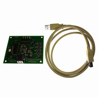
Manufacturer Part Number
MAX3420EEVKIT-2+
Description
EVAL KIT FOR MAX3420E
Manufacturer
Maxim Integrated Products
Specifications of MAX3420EEVKIT-2+
Main Purpose
Interface, USB 2.0 Slave
Embedded
No
Utilized Ic / Part
MAX3420E
Primary Attributes
Full Speed (12Mbps), SPI Interface, No Custom USB Drivers
Secondary Attributes
4 GPI Pushbuttons, 4 GPO LEDs
Lead Free Status / RoHS Status
Lead free / RoHS Compliant


The first five registers (R0–R4) access endpoint FIFOs.
To access a FIFO, an initial command byte sets the
register address and then consecutive reads or writes
keep the same register address to access subsequent
FIFO bytes.
The remaining registers (R5–R20) control the operation
of the MAX3420E. Once a register address above R4 is
set in the command byte, successive byte reads or
writes in the same SPI access cycle (SS low) increment
USB Peripheral Controller
with SPI Interface
Note: The acc (access) column indicates how the SPI master can access the register.
6
Table 1. MAX3420E Register Map
R EG
R10 C L R T O G S
R11 EPI R Q
R12 EPI EN
R13 U SB IR Q
R14 U SB IEN
R15 U SB C T L
R16 C PU C T L
R17 PIN C T L
R18 R EVISIO N
R19 F N A D D R
R20 IO PIN S
R0
R1
R2
R3
R4
R5
R6
R7
R8
R9
_______________________________________________________________________________________
EP0 F IF O
EP1 O U T F IF O
EP2 IN F IF O
EP3 IN F IF O
SU D F IF O
EP0 B C
EP1 O U T B C
EP2 IN B C
EP3 IN B C
EPST A L L S
R = read, RC = read or clear, RSC = read, set, or clear.
Writing to an R register (read only) has no effect.
Writing a 1 to an RC bit (read or clear) clears the bit.
Writing a zero to an RC bit has no effect.
NAME
U RE S D N IRQ V BU S IRQ N OV BU S IRQ S U S P IRQ
H OS C S TE N
U RE S D N IE
E P 3D IS AB
E P 3IN AK
GP IN 3
b 7
b 7
b 7
b 7
b 7
b 7
0
0
0
0
0
0
0
0
0
0
E P 2D IS AB
AC KS TAT
E P 2IN AK
V BG ATE
V BU S IE
GP IN 2
b 6
b 6
b 6
b 6
b 6
b 6
b 6
b 6
b 6
b 6
b 6
0
0
0
0
S U D AV IRQ IN 3BAV IRQ IN 2BAV IRQ OU T1D AV IRQ OU T0D AV IRQ IN 0BAV IRQ RC
N OV BU S IE
E P 1D IS AB
S U D AV IE
C H IP RE S
S TLS TAT
E P 0IN AK
GP IN 1
b 5
b 5
b 5
b 5
b 5
b 5
b 5
b 5
b 5
b 5
b 5
0
0
P WRD OWN C ON N E C T
C TG E P 3IN C TG E P 2IN C TG E P 1OU T
S TLE P 3IN
IN 3BAV IE
FD U P S P I
S U S P IE
GP IN 0
b 4
b 4
b 4
b 4
b 4
b 4
b 4
b 4
b 4
b 4
b 4
0
0
the register address after every byte read or written. This
incrementing operation continues until R20 is accessed.
Subsequent byte reads or writes continue to access
R20. Note that this autoincrementing action stops with
the next SPI cycle, which establishes a new register
address. Addressing beyond R20 is ignored.
The MAX3420E register map is depicted in Table 1. For
a complete description of all register contents, please
refer to the MAX3420E Programming Guide.
S TLE P 2IN
IN TLE V E L
IN 2BAV IE
U RE S IRQ
GP O U T3
U RE S IE
b 3
b 3
b 3
b 3
b 3
b 3
b 3
b 3
b 3
b 3
b 3
0
0
S TLE P 1OU T
BU S AC TIRQ
OU T1D AV IE
BU S AC TIE
GP O U T2
S IG RWU
P OS IN T
b 2
b 2
b 2
b 2
b 2
b 2
b 2
b 2
b 2
b 2
b 2
0
1
S TLE P 0OU T
OU T0D AV IE
RWU D N IRQ OS C OKIRQ RC
RWU D N IE
GP O U T1
GP X B
b 1
b 1
b 1
b 1
b 1
b 1
b 1
b 1
b 1
b 1
b 1
0
0
0
0
S TLE P 0IN RS C
OS C OKIE RS C
IN 0BAV IE RS C
GP O U T0
GP X A
b 0
b 0
b 0
b 0
b 0
b 0
b 0
b 0
b 0
b 0
b 0
IE
0
0
0
RS C
RS C
RS C
RS C
RS C
RS C
RS C
RS C
RS C
RS C
RS C
RS C
RS C
RS C
a c c
R
R
Related parts for MAX3420EEVKIT-2+
Image
Part Number
Description
Manufacturer
Datasheet
Request
R

Part Number:
Description:
MAX7528KCWPMaxim Integrated Products [CMOS Dual 8-Bit Buffered Multiplying DACs]
Manufacturer:
Maxim Integrated Products
Datasheet:
Part Number:
Description:
Single +5V, fully integrated, 1.25Gbps laser diode driver.
Manufacturer:
Maxim Integrated Products
Datasheet:
Part Number:
Description:
Single +5V, fully integrated, 155Mbps laser diode driver.
Manufacturer:
Maxim Integrated Products
Datasheet:
Part Number:
Description:
VRD11/VRD10, K8 Rev F 2/3/4-Phase PWM Controllers with Integrated Dual MOSFET Drivers
Manufacturer:
Maxim Integrated Products
Datasheet:
Part Number:
Description:
Highly Integrated Level 2 SMBus Battery Chargers
Manufacturer:
Maxim Integrated Products
Datasheet:
Part Number:
Description:
Current Monitor and Accumulator with Integrated Sense Resistor; ; Temperature Range: -40°C to +85°C
Manufacturer:
Maxim Integrated Products
Part Number:
Description:
TSSOP 14/A�/RS-485 Transceivers with Integrated 100O/120O Termination Resis
Manufacturer:
Maxim Integrated Products
Part Number:
Description:
TSSOP 14/A�/RS-485 Transceivers with Integrated 100O/120O Termination Resis
Manufacturer:
Maxim Integrated Products
Part Number:
Description:
QFN 16/A�/AC-DC and DC-DC Peak-Current-Mode Converters with Integrated Step
Manufacturer:
Maxim Integrated Products
Part Number:
Description:
TDFN/A/65V, 1A, 600KHZ, SYNCHRONOUS STEP-DOWN REGULATOR WITH INTEGRATED SWI
Manufacturer:
Maxim Integrated Products
Part Number:
Description:
Integrated Temperature Controller f
Manufacturer:
Maxim Integrated Products
Part Number:
Description:
SOT23-6/I�/45MHz to 650MHz, Integrated IF VCOs with Differential Output
Manufacturer:
Maxim Integrated Products
Part Number:
Description:
SOT23-6/I�/45MHz to 650MHz, Integrated IF VCOs with Differential Output
Manufacturer:
Maxim Integrated Products
Part Number:
Description:
EVALUATION KIT/2.4GHZ TO 2.5GHZ 802.11G/B RF TRANSCEIVER WITH INTEGRATED PA
Manufacturer:
Maxim Integrated Products
Part Number:
Description:
QFN/E/DUAL PCIE/SATA HIGH SPEED SWITCH WITH INTEGRATED BIAS RESISTOR
Manufacturer:
Maxim Integrated Products
Datasheet: