MCP1631RD-MCC2 Microchip Technology, MCP1631RD-MCC2 Datasheet - Page 86
MCP1631RD-MCC2
Manufacturer Part Number
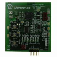
MCP1631RD-MCC2
Description
REFERENCE DESIGN MCP1631HV
Manufacturer
Microchip Technology
Datasheets
1.MCP1631VHVT-330EST.pdf
(34 pages)
2.MCP1631HV-330EST.pdf
(54 pages)
3.MCP1631RD-MCC2.pdf
(20 pages)
4.MCP1631RD-MCC2.pdf
(328 pages)
Specifications of MCP1631RD-MCC2
Main Purpose
Power Management, Battery Charger
Embedded
Yes, MCU, 8-Bit
Utilized Ic / Part
MCP1631HV, PIC16F883
Primary Attributes
1 ~ 2 Cell- Li-Ion, 1 ~ 5 Cell- NiCd/NiMH, 1 ~ 2 1W LEDs
Secondary Attributes
Status LEDs
Silicon Manufacturer
Microchip
Application Sub Type
Battery Charger
Kit Application Type
Power Management - Battery
Silicon Core Number
MCP1631HV, PIC16F883
Kit Contents
Board
Lead Free Status / RoHS Status
Lead free / RoHS Compliant
Lead Free Status / RoHS Status
Lead free / RoHS Compliant


PIC16F882/883/884/886/887
FIGURE 8-2:
FIGURE 8-3:
DS41291F-page 84
FixedRef
CV
C1R
FixedRef
CV
C2R
REF
REF
SEL
SEL
C12IN0-
C12IN1-
C12IN2-
C12IN3-
C2IN+
C12IN0-
C12IN1-
C12IN2-
C12IN3-
C1IN+
C2CH<1:0>
C1CH<1:0>
0
1
0
1
MUX
Note 1:
MUX
Note 1:
COMPARATOR C1 SIMPLIFIED BLOCK DIAGRAM
COMPARATOR C2 SIMPLIFIED BLOCK DIAGRAM
C1V
C1R
2:
3:
C2V
C2R
2:
3:
0
1
2
3
0
1
2
3
0
1
REF
2
MUX
0
1
REF
MUX
2
MUX
When C1ON = 0, the C1 comparator will produce a ‘0’ output to the XOR Gate.
Q1 and Q3 are phases of the four-phase system clock (F
Q1 is held high during Sleep mode.
MUX
When C2ON = 0, the C2 comparator will produce a ‘0’ output to the XOR Gate.
Q1 and Q3 are phases of the four-phase system clock (F
Q1 is held high during Sleep mode.
C2V
C2V
C1V
C1V
IN
IN
+
IN
IN
-
-
+
C2
C2ON
+
-
C1
C1ON
C2POL
(1)
C1POL
(1)
From Timer1
Q3*RD_CM2CON0
Clock
Q3*RD_CM1CON0
Q1
Q1
D
C2OUT
D
EN
Reset
D
EN
C1OUT
Reset
Q
Q
C2SYNC
Q
D
EN
C2POL
D
EN
CL
OSC
0
1
C1POL
OSC
MUX
CL
Q
Q
).
).
© 2009 Microchip Technology Inc.
To Timer1 Gate, SR Latch,
PWM Logic, and other
peripherals
RD_CM2CON0
RD_CM1CON0
C1OUT (to SR Latch)
To PWM Logic
SYNCC2OUT
Data Bus
Set C2IF
Data Bus
Set C1IF
To
To
Related parts for MCP1631RD-MCC2
Image
Part Number
Description
Manufacturer
Datasheet
Request
R

Part Number:
Description:
REFERENCE DESIGN FOR MCP1631HV
Manufacturer:
Microchip Technology
Datasheet:

Part Number:
Description:
REF DES BATT CHARG OR LED DRIVER
Manufacturer:
Microchip Technology
Datasheet:

Part Number:
Description:
Manufacturer:
Microchip Technology Inc.
Datasheet:
Part Number:
Description:
Manufacturer:
Microchip Technology Inc.
Datasheet:
Part Number:
Description:
Manufacturer:
Microchip Technology Inc.
Datasheet:
Part Number:
Description:
Manufacturer:
Microchip Technology Inc.
Datasheet:
Part Number:
Description:
Manufacturer:
Microchip Technology Inc.
Datasheet:
Part Number:
Description:
Manufacturer:
Microchip Technology Inc.
Datasheet:
Part Number:
Description:
Manufacturer:
Microchip Technology Inc.
Datasheet:
Part Number:
Description:
Manufacturer:
Microchip Technology Inc.
Datasheet: