MCP1631RD-MCC2 Microchip Technology, MCP1631RD-MCC2 Datasheet - Page 137
MCP1631RD-MCC2
Manufacturer Part Number
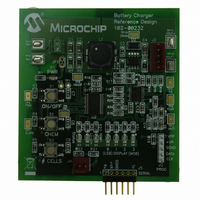
MCP1631RD-MCC2
Description
REFERENCE DESIGN MCP1631HV
Manufacturer
Microchip Technology
Datasheets
1.MCP1631VHVT-330EST.pdf
(34 pages)
2.MCP1631HV-330EST.pdf
(54 pages)
3.MCP1631RD-MCC2.pdf
(20 pages)
4.MCP1631RD-MCC2.pdf
(328 pages)
Specifications of MCP1631RD-MCC2
Main Purpose
Power Management, Battery Charger
Embedded
Yes, MCU, 8-Bit
Utilized Ic / Part
MCP1631HV, PIC16F883
Primary Attributes
1 ~ 2 Cell- Li-Ion, 1 ~ 5 Cell- NiCd/NiMH, 1 ~ 2 1W LEDs
Secondary Attributes
Status LEDs
Silicon Manufacturer
Microchip
Application Sub Type
Battery Charger
Kit Application Type
Power Management - Battery
Silicon Core Number
MCP1631HV, PIC16F883
Kit Contents
Board
Lead Free Status / RoHS Status
Lead free / RoHS Compliant
Lead Free Status / RoHS Status
Lead free / RoHS Compliant


11.6.1
In Half-Bridge mode, two pins are used as outputs to
drive push-pull loads. The PWM output signal is output
on the CCPx/P1A pin, while the complementary PWM
output signal is output on the P1B pin (see Figure 11-9).
This mode can be used for Half-Bridge applications, as
shown in Figure 11-9, or for Full-Bridge applications,
where four power switches are being modulated with
two PWM signals.
In Half-Bridge mode, the programmable dead-band delay
can be used to prevent shoot-through current in Half-
Bridge power devices. The value of the PDC<6:0> bits of
the PWM1CON register sets the number of instruction
cycles before the output is driven active. If the value is
greater than the duty cycle, the corresponding output
remains
Section 11.6.6 “Programmable Dead-Band Delay
Mode” for more details of the dead-band delay
operations.
FIGURE 11-9:
© 2009 Microchip Technology Inc.
Standard Half-Bridge Circuit (“Push-Pull”)
Half-Bridge Output Driving a Full-Bridge Circuit
inactive
HALF-BRIDGE MODE
during
EXAMPLE OF HALF-BRIDGE APPLICATIONS
the
P1A
P1B
entire
cycle.
P1A
P1B
FET
Driver
FET
Driver
PIC16F882/883/884/886/887
See
FET
Driver
FET
Driver
Since the P1A and P1B outputs are multiplexed with
the PORT data latches, the associated TRIS bits must
be cleared to configure P1A and P1B as outputs.
FIGURE 11-8:
P1A
P1B
td = Dead-Band Delay
Note 1: At this time, the TMR2 register is equal to the
Load
V+
(2)
(2)
2: Output signals are shown as active-high.
(1)
td
PR2 register.
Pulse Width
Load
Period
td
FET
Driver
FET
Driver
EXAMPLE OF HALF-
BRIDGE PWM OUTPUT
+
-
+
-
(1)
DS41291F-page 135
Period
(1)
Related parts for MCP1631RD-MCC2
Image
Part Number
Description
Manufacturer
Datasheet
Request
R

Part Number:
Description:
REFERENCE DESIGN FOR MCP1631HV
Manufacturer:
Microchip Technology
Datasheet:

Part Number:
Description:
REF DES BATT CHARG OR LED DRIVER
Manufacturer:
Microchip Technology
Datasheet:

Part Number:
Description:
Manufacturer:
Microchip Technology Inc.
Datasheet:
Part Number:
Description:
Manufacturer:
Microchip Technology Inc.
Datasheet:
Part Number:
Description:
Manufacturer:
Microchip Technology Inc.
Datasheet:
Part Number:
Description:
Manufacturer:
Microchip Technology Inc.
Datasheet:
Part Number:
Description:
Manufacturer:
Microchip Technology Inc.
Datasheet:
Part Number:
Description:
Manufacturer:
Microchip Technology Inc.
Datasheet:
Part Number:
Description:
Manufacturer:
Microchip Technology Inc.
Datasheet:
Part Number:
Description:
Manufacturer:
Microchip Technology Inc.
Datasheet: