MCP1631RD-MCC2 Microchip Technology, MCP1631RD-MCC2 Datasheet - Page 52
MCP1631RD-MCC2
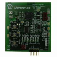
Manufacturer Part Number
MCP1631RD-MCC2
Description
REFERENCE DESIGN MCP1631HV
Manufacturer
Microchip Technology
Datasheets
1.MCP1631VHVT-330EST.pdf
(34 pages)
2.MCP1631HV-330EST.pdf
(54 pages)
3.MCP1631RD-MCC2.pdf
(20 pages)
4.MCP1631RD-MCC2.pdf
(328 pages)
Specifications of MCP1631RD-MCC2
Main Purpose
Power Management, Battery Charger
Embedded
Yes, MCU, 8-Bit
Utilized Ic / Part
MCP1631HV, PIC16F883
Primary Attributes
1 ~ 2 Cell- Li-Ion, 1 ~ 5 Cell- NiCd/NiMH, 1 ~ 2 1W LEDs
Secondary Attributes
Status LEDs
Silicon Manufacturer
Microchip
Application Sub Type
Battery Charger
Kit Application Type
Power Management - Battery
Silicon Core Number
MCP1631HV, PIC16F883
Kit Contents
Board
Lead Free Status / RoHS Status
Lead free / RoHS Compliant
Lead Free Status / RoHS Status
Lead free / RoHS Compliant


PIC16F882/883/884/886/887
3.4.4
Each PORTB pin is multiplexed with other functions. The
pins and their combined functions are briefly described
here. For specific information about individual functions
such as the SSP, I
section in this data sheet.
3.4.4.1
Figure 3-9 shows the diagram for this pin. This pin is
configurable to function as one of the following:
• a general purpose I/O
• an analog input for the ADC
• an external edge triggered interrupt
3.4.4.2
Figure 3-9 shows the diagram for this pin. This pin is
configurable to function as one of the following:
• a general purpose I/O
• an analog input for the ADC
• a PWM output
• an analog input to Comparator C1 or C2
3.4.4.3
Figure 3-9 shows the diagram for this pin. This pin is
configurable to function as one of the following:
• a general purpose I/O
• an analog input for the ADC
• a PWM output
3.4.4.4
Figure 3-9 shows the diagram for this pin. This pin is
configurable to function as one of the following:
• a general purpose I/O
• an analog input for the ADC
• Low-voltage In-Circuit Serial Programming enable
• an analog input to Comparator C1 or C2
DS41291F-page 50
pin
Note 1: P1C is available on PIC16F882/883/886
Note 1: P1B is available on PIC16F882/883/886
PIN DESCRIPTIONS AND
DIAGRAMS
only.
only.
RB0/AN12/INT
RB1/AN10/P1C
RB2/AN8/P1B
RB3/AN9/PGM/C12IN2-
(1)
(1)
2
C or interrupts, refer to the appropriate
(1)
(1)
/C12IN3-
FIGURE 3-9:
Data Bus
PORTB
PORTB
WPUB
WPUB
TRISB
TRISB
IOCB
IOCB
Interrupt-on-
WR
WR
WR
WR
RD
RD
RD
RD
Note 1:
Change
D
D
D
D
RB0/INT
RB3/PGM
To A/D Converter
To Comparator (RB1, RB3)
CK
CK
CK
CK
ANSELH determines Analog Input mode.
Q
Q
Q
Q
Q
Q
Q
Q
BLOCK DIAGRAM OF
RB<3:0>
CCP1OUT
Input Mode
RD PORTB
Analog
© 2009 Microchip Technology Inc.
CCP1OUT Enable
(1)
Input Mode
RBPU
Analog
1
0
Q
Q
(1)
EN
EN
D
D
V
DD
Weak
V
V
Q3
DD
SS
I/O Pin
Related parts for MCP1631RD-MCC2
Image
Part Number
Description
Manufacturer
Datasheet
Request
R

Part Number:
Description:
REFERENCE DESIGN FOR MCP1631HV
Manufacturer:
Microchip Technology
Datasheet:

Part Number:
Description:
REF DES BATT CHARG OR LED DRIVER
Manufacturer:
Microchip Technology
Datasheet:

Part Number:
Description:
Manufacturer:
Microchip Technology Inc.
Datasheet:
Part Number:
Description:
Manufacturer:
Microchip Technology Inc.
Datasheet:
Part Number:
Description:
Manufacturer:
Microchip Technology Inc.
Datasheet:
Part Number:
Description:
Manufacturer:
Microchip Technology Inc.
Datasheet:
Part Number:
Description:
Manufacturer:
Microchip Technology Inc.
Datasheet:
Part Number:
Description:
Manufacturer:
Microchip Technology Inc.
Datasheet:
Part Number:
Description:
Manufacturer:
Microchip Technology Inc.
Datasheet:
Part Number:
Description:
Manufacturer:
Microchip Technology Inc.
Datasheet: