MCP1631RD-MCC2 Microchip Technology, MCP1631RD-MCC2 Datasheet - Page 185
MCP1631RD-MCC2
Manufacturer Part Number
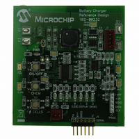
MCP1631RD-MCC2
Description
REFERENCE DESIGN MCP1631HV
Manufacturer
Microchip Technology
Datasheets
1.MCP1631VHVT-330EST.pdf
(34 pages)
2.MCP1631HV-330EST.pdf
(54 pages)
3.MCP1631RD-MCC2.pdf
(20 pages)
4.MCP1631RD-MCC2.pdf
(328 pages)
Specifications of MCP1631RD-MCC2
Main Purpose
Power Management, Battery Charger
Embedded
Yes, MCU, 8-Bit
Utilized Ic / Part
MCP1631HV, PIC16F883
Primary Attributes
1 ~ 2 Cell- Li-Ion, 1 ~ 5 Cell- NiCd/NiMH, 1 ~ 2 1W LEDs
Secondary Attributes
Status LEDs
Silicon Manufacturer
Microchip
Application Sub Type
Battery Charger
Kit Application Type
Power Management - Battery
Silicon Core Number
MCP1631HV, PIC16F883
Kit Contents
Board
Lead Free Status / RoHS Status
Lead free / RoHS Compliant
Lead Free Status / RoHS Status
Lead free / RoHS Compliant


13.3
The SPI mode allows 8 bits of data to be synchronously
transmitted and received, simultaneously. All four modes
of SPI are supported. To accomplish communication,
typically three pins are used:
• Serial Data Out (SDO) – RC5/SDO
• Serial Data In (SDI) – RC4/SDI/SDA
• Serial Clock (SCK) – RC3/SCK/SCL
Additionally, a fourth pin may be used when in any
Slave mode of operation:
• Slave Select (SS) – RA5/SS/AN4
13.3.1
When initializing the SPI, several options need to be
specified. This is done by programming the appropriate
control bits SSPCON<5:0> and SSPSTAT<7:6>.
These control bits allow the following to be specified:
• Master mode (SCK is the clock output)
• Slave mode (SCK is the clock input)
• Clock polarity (Idle state of SCK)
• Data input sample phase (middle or end of data
• Clock edge (output data on rising/falling edge of
• Clock rate (Master mode only)
• Slave Select mode (Slave mode only)
Figure 13-1 shows the block diagram of the MSSP
module, when in SPI mode.
© 2009 Microchip Technology Inc.
output time)
SCK)
SPI Mode
OPERATION
PIC16F882/883/884/886/887
FIGURE 13-1:
The MSSP consists of a transmit/receive shift register
(SSPSR) and a buffer register (SSPBUF). The SSPSR
shifts the data in and out of the device, MSb first. The
SSPBUF holds the data that was written to the SSPSR,
until the received data is ready. Once the 8 bits of data
have been received, that byte is moved to the SSPBUF
register. Then, the buffer full-detect bit BF of the SSP-
STAT register and the interrupt flag bit SSPIF of the
PIR1 register are set. This double buffering of the
received data (SSPBUF) allows the next byte to start
reception before reading the data that was just
received. Any write to the SSPBUF register during
transmission/reception of data will be ignored, and the
write collision detect bit WCOL of the SSPCON register
will be set. User software must clear the WCOL bit so
that it can be determined if the following write(s) to the
SSPBUF register completed successfully.
SDO
SCK
SDI
Note: I/O pins have diode protection to V
SS
Read
SS Control
Select
SMP:CKE
Edge
bit 0
Enable
Select
Edge
SSPBUF Reg
MSSP BLOCK DIAGRAM
(SPI MODE)
TRIS bit
Data to TX/RX in SSPSR
SSPSR Reg
2
SSPM<3:0>
Clock Select
4
2
DS41291F-page 183
(
Write
Prescaler
4, 16, 64
TMR2 Output
Clock
Shift
DD
Data Bus
Internal
and V
2
T
OSC
SS
)
.
Related parts for MCP1631RD-MCC2
Image
Part Number
Description
Manufacturer
Datasheet
Request
R

Part Number:
Description:
REFERENCE DESIGN FOR MCP1631HV
Manufacturer:
Microchip Technology
Datasheet:

Part Number:
Description:
REF DES BATT CHARG OR LED DRIVER
Manufacturer:
Microchip Technology
Datasheet:

Part Number:
Description:
Manufacturer:
Microchip Technology Inc.
Datasheet:
Part Number:
Description:
Manufacturer:
Microchip Technology Inc.
Datasheet:
Part Number:
Description:
Manufacturer:
Microchip Technology Inc.
Datasheet:
Part Number:
Description:
Manufacturer:
Microchip Technology Inc.
Datasheet:
Part Number:
Description:
Manufacturer:
Microchip Technology Inc.
Datasheet:
Part Number:
Description:
Manufacturer:
Microchip Technology Inc.
Datasheet:
Part Number:
Description:
Manufacturer:
Microchip Technology Inc.
Datasheet:
Part Number:
Description:
Manufacturer:
Microchip Technology Inc.
Datasheet: