MCP1631RD-MCC2 Microchip Technology, MCP1631RD-MCC2 Datasheet - Page 217
MCP1631RD-MCC2
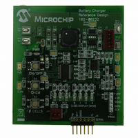
Manufacturer Part Number
MCP1631RD-MCC2
Description
REFERENCE DESIGN MCP1631HV
Manufacturer
Microchip Technology
Datasheets
1.MCP1631VHVT-330EST.pdf
(34 pages)
2.MCP1631HV-330EST.pdf
(54 pages)
3.MCP1631RD-MCC2.pdf
(20 pages)
4.MCP1631RD-MCC2.pdf
(328 pages)
Specifications of MCP1631RD-MCC2
Main Purpose
Power Management, Battery Charger
Embedded
Yes, MCU, 8-Bit
Utilized Ic / Part
MCP1631HV, PIC16F883
Primary Attributes
1 ~ 2 Cell- Li-Ion, 1 ~ 5 Cell- NiCd/NiMH, 1 ~ 2 1W LEDs
Secondary Attributes
Status LEDs
Silicon Manufacturer
Microchip
Application Sub Type
Battery Charger
Kit Application Type
Power Management - Battery
Silicon Core Number
MCP1631HV, PIC16F883
Kit Contents
Board
Lead Free Status / RoHS Status
Lead free / RoHS Compliant
Lead Free Status / RoHS Status
Lead free / RoHS Compliant


14.2.5
On power-up, the time-out sequence is as follows: first,
PWRT time-out is invoked after POR has expired, then
OST is activated after the PWRT time-out has expired.
The total time-out will vary based on oscillator
configuration and PWRTE bit status. For example, in
EC mode with PWRTE bit erased (PWRT disabled),
there will be no time-out at all. Figures 14-4, 14-5
and 14-6 depict time-out sequences. The device can
execute code from the INTOSC while OST is active by
enabling Two-Speed Start-up or Fail-Safe Monitor (see
Section 4.7.2 “Two-speed Start-up Sequence” and
Section 4.8 “Fail-Safe Clock Monitor”).
Since the time-outs occur from the POR pulse, if MCLR
is kept low long enough, the time-outs will expire. Then,
bringing MCLR high will begin execution immediately
(see Figure 14-5). This is useful for testing purposes or
to
PIC16F882/883/884/886/887 device operating in par-
allel.
Table 14-5 shows the Reset conditions for some
special registers, while Table 14-4 shows the Reset
conditions for all the registers.
TABLE 14-1:
TABLE 14-2:
TABLE 14-3:
© 2009 Microchip Technology Inc.
XT, HS, LP
LP, T1OSCIN = 1
RC, EC, INTOSC
PCON
STATUS
Legend:
Note
Legend: u = unchanged, x = unknown
Oscillator Configuration
POR
Name
0
u
u
u
u
u
1:
synchronize
u = unchanged, x = unknown, — = unimplemented bit, reads as ‘0’, q = value depends on condition. Shaded cells are not used by BOR.
Other (non Power-up) Resets include MCLR Reset and Watchdog Timer Reset during normal operation.
TIME-OUT SEQUENCE
BOR
Bit 7
x
0
u
u
u
u
IRP
—
TIME-OUT IN VARIOUS SITUATIONS
STATUS/PCON BITS AND THEIR SIGNIFICANCE
SUMMARY OF REGISTERS ASSOCIATED WITH BROWN-OUT
Bit 6
RP1
TO
—
1
1
0
0
u
1
more
PWRTE = 0
1024 • T
ULPWUE
T
T
T
PWRT
Bit 5
RPO
PWRT
PWRT
PD
1
1
u
0
u
0
than
OSC
+
Power-up
SBOREN
Bit 4
Power-on Reset
Brown-out Reset
WDT Reset
WDT Wake-up
MCLR Reset during normal operation
MCLR Reset during Sleep
TO
PIC16F882/883/884/886/887
PWRTE = 1
1024 • T
one
Bit 3
—
—
PD
—
OSC
14.2.6
The Power Control register PCON (address 8Eh) has
two Status bits to indicate what type of Reset that last
occurred.
Bit 0 is BOR (Brown-out Reset). BOR is unknown on
Power-on Reset. It must then be set by the user and
checked on subsequent Resets to see if BOR = 0,
indicating that a Brown-out has occurred. The BOR
Status bit is a “don’t care” and is not necessarily
predictable if the brown-out circuit is disabled
(BOREN<1:0>
Register 1).
Bit 1 is POR (Power-on Reset). It is a ‘0’ on Power-on
Reset and unaffected otherwise. The user must write a
‘1’ to this bit following a Power-on Reset. On a
subsequent Reset, if POR is ‘0’, it will indicate that a
Power-on Reset has occurred (i.e., V
gone too low).
For more information, see Section 3.2.2 “Ultra
Low-Power
“Brown-out Reset (BOR)”.
Bit 2
—
Z
PWRTE = 0
1024 • T
T
T
T
PWRT
PWRT
PWRT
Brown-out Reset
Bit 1
POR
DC
POWER CONTROL (PCON)
REGISTER
Condition
OSC
+
Wake-up”
= 00 in the Configuration Word
Bit 0
BOR
C
1024 • T
PWRTE = 1
—
—
--01 --qq
0001 1xxx
POR, BOR
OSC
Value on
and
DS41291F-page 215
Wake-up from
Section 14.2.4
1024 • T
DD
Sleep
--0u --uu
000q quuu
may have
Value on
—
—
all other
Resets
OSC
Related parts for MCP1631RD-MCC2
Image
Part Number
Description
Manufacturer
Datasheet
Request
R

Part Number:
Description:
REFERENCE DESIGN FOR MCP1631HV
Manufacturer:
Microchip Technology
Datasheet:

Part Number:
Description:
REF DES BATT CHARG OR LED DRIVER
Manufacturer:
Microchip Technology
Datasheet:

Part Number:
Description:
Manufacturer:
Microchip Technology Inc.
Datasheet:
Part Number:
Description:
Manufacturer:
Microchip Technology Inc.
Datasheet:
Part Number:
Description:
Manufacturer:
Microchip Technology Inc.
Datasheet:
Part Number:
Description:
Manufacturer:
Microchip Technology Inc.
Datasheet:
Part Number:
Description:
Manufacturer:
Microchip Technology Inc.
Datasheet:
Part Number:
Description:
Manufacturer:
Microchip Technology Inc.
Datasheet:
Part Number:
Description:
Manufacturer:
Microchip Technology Inc.
Datasheet:
Part Number:
Description:
Manufacturer:
Microchip Technology Inc.
Datasheet: