MCP1631RD-MCC2 Microchip Technology, MCP1631RD-MCC2 Datasheet - Page 178
MCP1631RD-MCC2
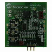
Manufacturer Part Number
MCP1631RD-MCC2
Description
REFERENCE DESIGN MCP1631HV
Manufacturer
Microchip Technology
Datasheets
1.MCP1631VHVT-330EST.pdf
(34 pages)
2.MCP1631HV-330EST.pdf
(54 pages)
3.MCP1631RD-MCC2.pdf
(20 pages)
4.MCP1631RD-MCC2.pdf
(328 pages)
Specifications of MCP1631RD-MCC2
Main Purpose
Power Management, Battery Charger
Embedded
Yes, MCU, 8-Bit
Utilized Ic / Part
MCP1631HV, PIC16F883
Primary Attributes
1 ~ 2 Cell- Li-Ion, 1 ~ 5 Cell- NiCd/NiMH, 1 ~ 2 1W LEDs
Secondary Attributes
Status LEDs
Silicon Manufacturer
Microchip
Application Sub Type
Battery Charger
Kit Application Type
Power Management - Battery
Silicon Core Number
MCP1631HV, PIC16F883
Kit Contents
Board
Lead Free Status / RoHS Status
Lead free / RoHS Compliant
Lead Free Status / RoHS Status
Lead free / RoHS Compliant


PIC16F882/883/884/886/887
12.4.2.3
The operation of the Synchronous Master and Slave
modes is identical (Section 12.4.1.5 “Synchronous
Master Reception”), with the following exceptions:
• Sleep
• CREN bit is always set, therefore the receiver is
• SREN bit, which is a “don't care” in Slave mode
A character may be received while in Sleep mode by
setting the CREN bit prior to entering Sleep. Once the
word is received, the RSR register will transfer the data
to the RCREG register. If the RCIE enable bit is set, the
interrupt generated will wake the device from Sleep
and execute the next instruction. If the GIE bit is also
set, the program will branch to the interrupt vector.
TABLE 12-10: REGISTERS ASSOCIATED WITH SYNCHRONOUS SLAVE RECEPTION
DS41291F-page 176
BAUDCTL ABDOVF
INTCON
PIE1
PIR1
RCREG
RCSTA
SPBRG
SPBRGH
TRISC
TXREG
TXSTA
Legend:
never Idle
Name
x = unknown, – = unimplemented read as ‘0’. Shaded cells are not used for Synchronous Slave Reception.
EUSART Receive Data Register
EUSART Transmit Data Register
TRISC7
BRG15
SPEN
BRG7
CSRC
EUSART Synchronous Slave
Reception
Bit 7
GIE
—
—
TRISC6
BRG14
RCIDL
BRG6
PEIE
ADIE
ADIF
Bit 6
RX9
TX9
TRISC5
BRG13
SREN
BRG5
TXEN
RCIE
RCIF
Bit 5
T0IE
—
TRISC4
BRG12
CREN
SYNC
SCKP
BRG4
INTE
Bit 4
TXIE
TXIF
ADDEN
TRISC3
SENDB
BRG16
BRG11
SSPIE
SSPIF
BRG3
RBIE
Bit 3
CCP1IE
CCP1IF
TRISC2
BRG10
FERR
BRGH
BRG2
12.4.2.4
1.
2.
3.
4.
5.
6.
7.
8.
Bit 2
T0IF
—
Set the SYNC and SPEN bits and clear the
CSRC bit.
If interrupts are desired, set the RCIE bit of the
PIE1 register and the GIE and PEIE bits of the
INTCON register.
If 9-bit reception is desired, set the RX9 bit.
Set the CREN bit to enable reception.
The RCIF bit will be set when reception is
complete. An interrupt will be generated if the
RCIE bit was set.
If 9-bit mode is enabled, retrieve the Most
Significant bit from the RX9D bit of the RCSTA
register.
Retrieve the 8 Least Significant bits from the
receive FIFO by reading the RCREG register.
If an overrun error occurs, clear the error by
either clearing the CREN bit of the RCSTA
register or by clearing the SPEN bit which resets
the EUSART.
TMR2IE
TMR2IF
TRISC1
OERR
TRMT
BRG1
BRG9
WUE
Bit 1
INTF
Synchronous Slave Reception Set-
up:
TMR1IE
TMR1IF
TRISC0
ABDEN
RX9D
BRG0
BRG8
TX9D
Bit 0
RBIF
© 2009 Microchip Technology Inc.
01-0 0-00
0000 000x
-000 0000
-000 0000
0000 0000
0000 000x
0000 0000
0000 0000
1111 1111
0000 0000
0000 0010
POR, BOR
Value on
01-0 0-00
0000 000x
-000 0000
-000 0000
0000 0000
0000 000x
0000 0000
0000 0000
1111 1111
0000 0000
0000 0010
Value on
all other
Resets
Related parts for MCP1631RD-MCC2
Image
Part Number
Description
Manufacturer
Datasheet
Request
R

Part Number:
Description:
REFERENCE DESIGN FOR MCP1631HV
Manufacturer:
Microchip Technology
Datasheet:

Part Number:
Description:
REF DES BATT CHARG OR LED DRIVER
Manufacturer:
Microchip Technology
Datasheet:

Part Number:
Description:
Manufacturer:
Microchip Technology Inc.
Datasheet:
Part Number:
Description:
Manufacturer:
Microchip Technology Inc.
Datasheet:
Part Number:
Description:
Manufacturer:
Microchip Technology Inc.
Datasheet:
Part Number:
Description:
Manufacturer:
Microchip Technology Inc.
Datasheet:
Part Number:
Description:
Manufacturer:
Microchip Technology Inc.
Datasheet:
Part Number:
Description:
Manufacturer:
Microchip Technology Inc.
Datasheet:
Part Number:
Description:
Manufacturer:
Microchip Technology Inc.
Datasheet:
Part Number:
Description:
Manufacturer:
Microchip Technology Inc.
Datasheet: