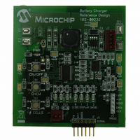
MCP1631RD-MCC2 Microchip Technology, MCP1631RD-MCC2 Datasheet - Page 253

MCP1631RD-MCC2
Manufacturer Part Number
MCP1631RD-MCC2
Description
REFERENCE DESIGN MCP1631HV
Manufacturer
Microchip Technology
Datasheets
1.MCP1631VHVT-330EST.pdf
(34 pages)
2.MCP1631HV-330EST.pdf
(54 pages)
3.MCP1631RD-MCC2.pdf
(20 pages)
4.MCP1631RD-MCC2.pdf
(328 pages)
Specifications of MCP1631RD-MCC2
Main Purpose
Power Management, Battery Charger
Embedded
Yes, MCU, 8-Bit
Utilized Ic / Part
MCP1631HV, PIC16F883
Primary Attributes
1 ~ 2 Cell- Li-Ion, 1 ~ 5 Cell- NiCd/NiMH, 1 ~ 2 1W LEDs
Secondary Attributes
Status LEDs
Silicon Manufacturer
Microchip
Application Sub Type
Battery Charger
Kit Application Type
Power Management - Battery
Silicon Core Number
MCP1631HV, PIC16F883
Kit Contents
Board
Lead Free Status / RoHS Status
Lead free / RoHS Compliant
Lead Free Status / RoHS Status
Lead free / RoHS Compliant
- MCP1631VHVT-330EST PDF datasheet
- MCP1631HV-330EST PDF datasheet #2
- MCP1631RD-MCC2 PDF datasheet #3
- MCP1631RD-MCC2 PDF datasheet #4
- Current page: 253 of 328
- Download datasheet (6Mb)
17.5
© 2009 Microchip Technology Inc.
DC CHARACTERISTICS
D030
D030A
D031
D032
D033
D033A
D040
D040A
D041
D042
D043
D043A
D043B
D060
D061
D063
D070*
D080
D090
Note 1:
Param
No.
2:
3:
4:
5:
*
†
V
V
I
I
V
V
DC Characteristics:
IL
PUR
IL
IH
OL
OH
Sym.
These parameters are characterized but not tested.
Data in “Typ” column is at 5.0V, 25°C unless otherwise stated. These parameters are for design guidance only and are
not tested.
In RC oscillator configuration, the OSC1/CLKIN pin is a Schmitt Trigger input. It is not recommended to use an external
clock in RC mode.
Negative current is defined as current sourced by the pin.
The leakage current on the MCLR pin is strongly dependent on the applied voltage level. The specified levels represent
normal operating conditions. Higher leakage current may be measured at different input voltages.
See Section 10.3.1 “Using the Data EEPROM” for additional information.
Including OSC2 in CLKOUT mode.
Input Low Voltage
I/O Port:
MCLR, OSC1 (RC mode)
OSC1 (XT and LP modes)
OSC1 (HS mode)
Input High Voltage
I/O ports:
MCLR
OSC1 (XT and LP modes)
OSC1 (HS mode)
OSC1 (RC mode)
Input Leakage Current
I/O ports
MCLR
OSC1
PORTB Weak Pull-up Current
Output Low Voltage
I/O ports
Output High Voltage
I/O ports
with TTL buffer
with TTL buffer
with Schmitt Trigger buffer
with Schmitt Trigger buffer
(3)
Characteristic
(5)
(5)
(2)
PIC16F883/884/886/887-I (Industrial)
PIC16F883/884/886/887-E (Extended)
(1)
PIC16F882/883/884/886/887
Standard Operating Conditions (unless otherwise stated)
Operating temperature
0.25 V
V
0.8 V
0.8 V
0.7 V
0.9 V
DD
Min.
V
V
V
Vss
Vss
Vss
2.0
1.6
50
—
—
—
—
DD
SS
SS
SS
– 0.7
DD
DD
DD
DD
+ 0.8
Typ†
± 0.1
± 0.1
± 0.1
250
—
—
—
—
—
—
—
—
—
—
—
—
—
—
—
—
0.15 V
0.2 V
0.2 V
0.3 V
Max.
V
V
V
V
V
V
V
400
0.8
0.3
± 1
± 5
± 5
0.6
—
-40°C ≤ T
-40°C ≤ T
DD
DD
DD
DD
DD
DD
DD
DD
DD
DD
DD
Units
μA
μA
μA
μA
V
V
V
V
V
V
V
V
V
V
V
V
V
V
V
A
A
≤ +85°C for industrial
≤ +125°C for extended
4.5V ≤ V
2.0V ≤ V
2.0V ≤ V
4.5V ≤ V
2.0V ≤ V
2.0V ≤ V
(Note 1)
V
Pin at high-impedance
V
V
LP oscillator configuration
V
I
I
OL
OH
SS
SS
SS
DD
= 8.5 mA, V
= -3.0 mA, V
≤ V
≤ V
≤ V
= 5.0V, V
PIN
PIN
PIN
DD
DD
DD
DD
DD
DD
Conditions
≤ V
≤ V
≤ V
≤ 5.5V
≤ 4.5V
≤ 5.5V
≤ 5.5V
≤ 4.5V
≤ 5.5V
DS41291F-page 251
PIN
DD
DD
DD
DD
DD
,
, XT, HS and
= V
= 4.5V (Ind.)
= 4.5V (Ind.)
SS
Related parts for MCP1631RD-MCC2
Image
Part Number
Description
Manufacturer
Datasheet
Request
R

Part Number:
Description:
REFERENCE DESIGN FOR MCP1631HV
Manufacturer:
Microchip Technology
Datasheet:

Part Number:
Description:
REF DES BATT CHARG OR LED DRIVER
Manufacturer:
Microchip Technology
Datasheet:

Part Number:
Description:
Manufacturer:
Microchip Technology Inc.
Datasheet:

Part Number:
Description:
Manufacturer:
Microchip Technology Inc.
Datasheet:

Part Number:
Description:
Manufacturer:
Microchip Technology Inc.
Datasheet:

Part Number:
Description:
Manufacturer:
Microchip Technology Inc.
Datasheet:

Part Number:
Description:
Manufacturer:
Microchip Technology Inc.
Datasheet:

Part Number:
Description:
Manufacturer:
Microchip Technology Inc.
Datasheet:

Part Number:
Description:
Manufacturer:
Microchip Technology Inc.
Datasheet:

Part Number:
Description:
Manufacturer:
Microchip Technology Inc.
Datasheet:


