MCP1631RD-MCC2 Microchip Technology, MCP1631RD-MCC2 Datasheet - Page 102
MCP1631RD-MCC2
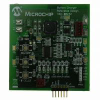
Manufacturer Part Number
MCP1631RD-MCC2
Description
REFERENCE DESIGN MCP1631HV
Manufacturer
Microchip Technology
Datasheets
1.MCP1631VHVT-330EST.pdf
(34 pages)
2.MCP1631HV-330EST.pdf
(54 pages)
3.MCP1631RD-MCC2.pdf
(20 pages)
4.MCP1631RD-MCC2.pdf
(328 pages)
Specifications of MCP1631RD-MCC2
Main Purpose
Power Management, Battery Charger
Embedded
Yes, MCU, 8-Bit
Utilized Ic / Part
MCP1631HV, PIC16F883
Primary Attributes
1 ~ 2 Cell- Li-Ion, 1 ~ 5 Cell- NiCd/NiMH, 1 ~ 2 1W LEDs
Secondary Attributes
Status LEDs
Silicon Manufacturer
Microchip
Application Sub Type
Battery Charger
Kit Application Type
Power Management - Battery
Silicon Core Number
MCP1631HV, PIC16F883
Kit Contents
Board
Lead Free Status / RoHS Status
Lead free / RoHS Compliant
Lead Free Status / RoHS Status
Lead free / RoHS Compliant


PIC16F882/883/884/886/887
9.1
When configuring and using the ADC the following
functions must be considered:
• Port configuration
• Channel selection
• ADC voltage reference selection
• ADC conversion clock source
• Interrupt control
• Results formatting
9.1.1
The ADC can be used to convert both analog and digital
signals. When converting analog signals, the I/O pin
should be configured for analog by setting the associated
TRIS and ANSEL bits. See the corresponding Port
section for more information.
9.1.2
The CHS bits of the ADCON0 register determine which
channel is connected to the sample and hold circuit.
When changing channels, a delay is required before
starting the next conversion. Refer to Section 9.2
“ADC Operation” for more information.
DS41291F-page 100
Note:
ADC Configuration
PORT CONFIGURATION
Analog voltages on any pin that is defined
as a digital input may cause the input
buffer to conduct excess current.
CHANNEL SELECTION
9.1.3
The VCFG bits of the ADCON0 register provide
independent control of the positive and negative
voltage references. The positive voltage reference can
be either V
the negative voltage reference can be either V
external voltage source.
9.1.4
The source of the conversion clock is software select-
able via the ADCS bits of the ADCON0 register. There
are four possible clock options:
• F
• F
• F
• F
The time to complete one bit conversion is defined as
T
as shown in Figure 9-2.
For correct conversion, the appropriate T
must be met. See A/D conversion requirements in
Section 17.0 “Electrical Specifications” for more
information. Table 9-1 gives examples of appropriate
ADC clock selections.
AD
Note:
OSC
OSC
OSC
RC
. One full 10-bit conversion requires 11 T
(dedicated internal oscillator)
/2
/8
/32
DD
ADC V
Unless using the F
system clock frequency will change the
ADC
adversely affect the ADC result.
CONVERSION CLOCK
or an external voltage source. Likewise,
clock
OLTAGE REFERENCE
© 2009 Microchip Technology Inc.
frequency,
RC
, any changes in the
AD
which
specification
AD
SS
periods
or an
may
Related parts for MCP1631RD-MCC2
Image
Part Number
Description
Manufacturer
Datasheet
Request
R

Part Number:
Description:
REFERENCE DESIGN FOR MCP1631HV
Manufacturer:
Microchip Technology
Datasheet:

Part Number:
Description:
REF DES BATT CHARG OR LED DRIVER
Manufacturer:
Microchip Technology
Datasheet:

Part Number:
Description:
Manufacturer:
Microchip Technology Inc.
Datasheet:
Part Number:
Description:
Manufacturer:
Microchip Technology Inc.
Datasheet:
Part Number:
Description:
Manufacturer:
Microchip Technology Inc.
Datasheet:
Part Number:
Description:
Manufacturer:
Microchip Technology Inc.
Datasheet:
Part Number:
Description:
Manufacturer:
Microchip Technology Inc.
Datasheet:
Part Number:
Description:
Manufacturer:
Microchip Technology Inc.
Datasheet:
Part Number:
Description:
Manufacturer:
Microchip Technology Inc.
Datasheet:
Part Number:
Description:
Manufacturer:
Microchip Technology Inc.
Datasheet: