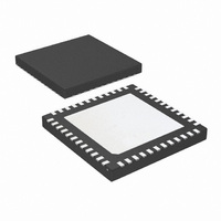
LM96194CISQ/NOPB National Semiconductor, LM96194CISQ/NOPB Datasheet - Page 25

LM96194CISQ/NOPB
Manufacturer Part Number
LM96194CISQ/NOPB
Description
IC TRUTHERM HDWR MONITOR 48-LLP
Manufacturer
National Semiconductor
Series
PowerWise®, TruTherm®r
Datasheet
1.LM96194CISQNOPB.pdf
(106 pages)
Specifications of LM96194CISQ/NOPB
Function
Fan Control, Temp Monitor
Topology
ADC (Sigma Delta), Comparator, Fan Control, Multiplexer, Register Bank
Sensor Type
External & Internal
Sensing Temperature
-40°C ~ 85°C, External Sensor
Output Type
SMBus™
Output Alarm
No
Output Fan
Yes
Voltage - Supply
3 V ~ 3.6 V
Operating Temperature
-40°C ~ 85°C
Mounting Type
Surface Mount
Package / Case
48-LLP
Lead Free Status / RoHS Status
Lead free / RoHS Compliant
Other names
LM96194CISQTR
14.5.4.6 I
The LM96194 supports I
1.
2.
3.
4.
5.
6.
7.
8.
9.
10. The master receives the last byte.
11. The master asserts a NACK.
12. The master issues a STOP.
Special Notes:
1.
2.
3.
4.
14.6 READING AND WRITING 16-BIT REGISTERS
Whenever the low byte of a 16-bit register is read, the high
byte is frozen. After the high byte is read, it is unfrozen. This
ensures that the entire 16-bit value is read properly and the
high byte matches with the low byte. If the low byte of a dif-
ferent 16-bit register is read, the currently frozen high byte is
unfrozen and the high byte of the new 16-bit register is frozen.
In a system with two SMBus masters, it is very important that
only one master reads any 16-bit registers at a time. One
possible method to achieve this would involve using 16-bit
SMBus reads (instead of two separate 8-bit reads) to read 16-
bit registers.
Whenever the low byte of a 16-bit register is written, the write
is buffered and does not take effect until the corresponding
high byte is written. If the low byte of a different 16-bit register
is written, the previously buffered low byte of the first register
is discarded. If a device attempts to write the high byte of a
16-bit register, and the corresponding low byte was not written
(or was discarded), then the LM96194 will NACK the byte.
15.0 Using The LM96194
15.1 POWER ON
The LM96194 generates a power on reset signal on RESET
when power is applied for the first time to the part.
15.2 RESETS
Upon power up, the RESET output is asserted when the volt-
age on the power supply crosses the power-on-reset thresh-
old level (see Electrical Specifications). The RESET output is
open-drain and should be used with an external pull-up re-
sistor connected to V
pleted, the RESET pin becomes an input and 10 µs after
assertion of RESET the LOCK bit in the LM96194 Configu-
ration register shall be cleared. In addition, 10 µs after asser-
1
S
The master sends a START to start this transaction .
The master send 7-bit slave address followed by a write bit (low).
The slave asserts an ACK.
The master sends the register address and the slave asserts an ACK.
The master sends a repeated START.
The master sends the 7-bit slave address followed by a read bit (high).
The slave asserts an ACK.
The master receives Data Byte 1 and asserts an ACK.
The master continues to receive bytes and asserting an ACK for each byte received.
The LM96194 returns 00h when address locations outside of normal address space are read.
Block reads do not wrap around from address FFh to 00h.
If the master acknowledges more bytes that it requested, the LM96194 continues to supply data until the master does not
acknowledge a byte.
If the master does not acknowledges a byte to prematurely abort a block read, the LM96194 gets off the bus to allow the
master to issue a STOP signal.
2
Slave
Address
2
C Block Reads
W
DD
3
A
. Once the power on reset has com-
2
C block reads. The following sequence of events occur in this transaction:
4
Register
Address
A
5
S
6
Slave
Address
R
25
7
A
tion of RESET the sleep control register shall be automatically
set to S4/S5. This causes several error events to be masked
according to the S4/S5 masking definitions. Since the RE-
SET pin becomes an active input, it must not be left floating
at any time as this may cause the LM96194 to drift into S4/S5
and thus have unpredictable behavior. RESET must be as-
serted for more than 4µs in order to guarantee detection.
All other registers are not effected by power on reset or ex-
ternal reset.
15.3 ADDRESS SELECTION
LM96194 is designed to be used primarily in dual processor
server systems that may require only one monitoring device.
If multiple LM96194 devices are implemented in a system,
they must have unique SMBus slave addresses. See the
Section 14.1 SMBus ADDRESSING
Factory regs
BMC Error Status regs
Host Error Status regs
Value regs
Limit regs
Setup regs
LM96194 Configuration Lock Bit
LM96194 Configuration GMSK
Bit
Sleep Mask
Sleep State Control
Other Mask regs
8
Data
Byte 1
Register Types
A
9
Data
Byte 2
A
… 10
… Data
On Reset
x (reset)
Power
for more information.
Byte N
x
x
x
x
x
x
x
x
www.national.com
External
11 12
/A
Reset
x
x
P


