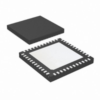
LM96194CISQ/NOPB National Semiconductor, LM96194CISQ/NOPB Datasheet - Page 13

LM96194CISQ/NOPB
Manufacturer Part Number
LM96194CISQ/NOPB
Description
IC TRUTHERM HDWR MONITOR 48-LLP
Manufacturer
National Semiconductor
Series
PowerWise®, TruTherm®r
Datasheet
1.LM96194CISQNOPB.pdf
(106 pages)
Specifications of LM96194CISQ/NOPB
Function
Fan Control, Temp Monitor
Topology
ADC (Sigma Delta), Comparator, Fan Control, Multiplexer, Register Bank
Sensor Type
External & Internal
Sensing Temperature
-40°C ~ 85°C, External Sensor
Output Type
SMBus™
Output Alarm
No
Output Fan
Yes
Voltage - Supply
3 V ~ 3.6 V
Operating Temperature
-40°C ~ 85°C
Mounting Type
Surface Mount
Package / Case
48-LLP
Lead Free Status / RoHS Status
Lead free / RoHS Compliant
Other names
LM96194CISQTR
12.6 RECOMMENDED EXTERNAL SCALING RESISTORS
FOR +12V POWER RAILS
The +12V inputs require external scaling resistors. The resis-
tors need to scale 12V down to 0.927V.
To calculate the required ratio of R1 to R2 use this equation:
It is recommended that the equivalent thevenin resistance of
the divider be between 1k and 7k to minimize errors caused
by leakage currents at extreme temperatures. The best val-
ues for the resistors are: R1=13.7 kΩ and R2=1.15 kΩ. This
yields a ratio of 11.94498, which has a +0.27% deviation from
the theoretical. It is also recommended that the resistors have
±1% tolerance or better.
Each LSB in the voltage value registers has a weight of 12V /
192 = 62.5 mV. To calculate the actual voltage of the +12V
power input, use the following equation:
12.7 RECOMMENDED EXTERNAL SCALING CIRCUIT
FOR −12V POWER INPUT
The −12V input requires external resistors to level shift the
nominal input voltage of −12V to +0.309V.
The +3.3V standby voltage is used as a reference for the level
shifting. Therefore, the tolerance of this voltage directly ef-
fects the accuracy of the −12V reading. To minimize ratio
errors, a tolerance of better than ±1% should be used. It is
recommended that the equivalent thevenin resistance of the
divider is between 1k and 7k to minimize errors caused by
leakage currents at extreme temperatures. To calculate the
ratio of R1 to R2 use this equation:
where V
reference voltage of +3.3V and AD_IN is the voltage required
at the AD input for a ¼ scale reading or 0.309V.
Therefore, for this case:
V
IN
FIGURE 3. Required External Level Shifting
IN
= (8-bit value register code) x (62.5 mV)
FIGURE 2. Required External Scaling
is the nominal input voltage of −12V, V
Resistors for +12V Power Input
Resistors for −12V Power Input
20194410
20194408
REF
is the
(1)
(2)
(3)
13
Using standard 1% resistor values for R1 of 5.76 kΩ and R2
of 1.4 kΩ yields an R1 to R2 ratio of 4.1143.
The input voltage V
ister reading (VR) using this equation:
The table below summarizes the theoretical voltage values
for value register readings near −12V.
Value Register
15
16
17
18
19
20
21
22
23
24
25
26
27
28
29
30
31
32
33
34
35
36
37
38
39
40
41
42
43
44
45
46
47
48
49
50
51
52
53
IN
can be calculated using the value reg-
-13.2068
-13.1821
-13.1574
-13.1327
-13.1080
-13.0833
-13.0586
-13.0339
-13.0092
-12.9845
-12.9598
-12.9351
-12.9104
-12.8858
-12.8611
-12.8364
-12.8117
-12.7870
-12.7623
-12.7376
-12.7129
-12.6882
-12.6635
-12.6388
-12.6141
-12.5894
-12.5648
-12.5401
-12.5154
-12.4907
-12.4660
-12.4413
-12.4166
-12.3919
-12.3672
-12.3425
-12.3178
-12.2931
-12.2684
V
IN
% Δ from −12V
-10.0563
-9.8505
-9.6448
-9.4390
-9.2332
-9.0275
-8.8217
-8.6159
-8.4101
-8.2044
-7.9986
-7.7928
-7.5871
-7.3813
-7.1755
-6.9698
-6.7640
-6.5582
-6.3524
-6.1467
-5.9409
-5.7351
-5.5294
-5.3236
-5.1178
-4.9121
-4.7063
-4.5005
-4.2947
-4.0890
-3.8832
-3.6774
-3.4717
-3.2659
-3.0601
-2.8544
-2.6486
-2.4428
-2.2370
www.national.com
(4)
(5)


