DS3170+ Maxim Integrated Products, DS3170+ Datasheet - Page 7
DS3170+
Manufacturer Part Number
DS3170+
Description
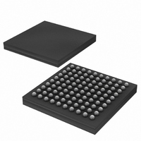
IC TXRX DS3/E3 100-CSBGA
Manufacturer
Maxim Integrated Products
Datasheet
1.DS3170.pdf
(230 pages)
Specifications of DS3170+
Function
Single-Chip Transceiver
Interface
DS3, E3
Number Of Circuits
1
Voltage - Supply
3.135 V ~ 3.465 V
Current - Supply
120mA
Operating Temperature
0°C ~ 70°C
Mounting Type
Surface Mount
Package / Case
100-LBGA
Includes
DS3 Framers, E3 Framers, HDLC Controller, On-Chip BERTs
Lead Free Status / RoHS Status
Lead free / RoHS Compliant
Power (watts)
-


DS3170 DS3/E3 Single-Chip Transceiver
Figure 10-13. DS3 Frame Format ........................................................................................................................ 81
Figure 10-14. DS3 Subframe Framer State Diagram ............................................................................................ 81
Figure 10-15. DS3 Multiframe Framer State Diagram ........................................................................................... 82
Figure 10-16. G.751 E3 Frame Format ................................................................................................................. 89
Figure 10-17. G.832 E3 Frame Format ................................................................................................................. 92
Figure 10-18. MA Byte Format ............................................................................................................................. 92
Figure 10-19. HDLC Controller Block Diagram ..................................................................................................... 97
Figure 10-20. Trail Trace Controller Block Diagram ............................................................................................ 100
Figure 10-21. Trail Trace Byte (DT = Trail Trace Data) ....................................................................................... 102
Figure 10-22. FEAC Controller Block Diagram ................................................................................................... 103
Figure 10-23. FEAC Codeword Format .............................................................................................................. 104
Figure 10-24. Line Encoder/Decoder Block Diagram .......................................................................................... 105
Figure 10-25. B3ZS Signatures .......................................................................................................................... 107
Figure 10-26. HDB3 Signatures ......................................................................................................................... 107
Figure 10-27. BERT Block Diagram ................................................................................................................... 108
Figure 10-28. PRBS Synchronization State Diagram .......................................................................................... 110
Figure 10-29. Repetitive Pattern Synchronization State Diagram ........................................................................ 111
Figure 10-30. LIU Functional Diagram ................................................................................................................ 112
Figure 10-31. DS3/E3 LIU Block Diagram .......................................................................................................... 113
Figure 10-32. Receiver Jitter Tolerance .............................................................................................................. 116
Figure 13-1. JTAG Block Diagram ...................................................................................................................... 202
Figure 13-2. JTAG TAP Controller State Machine .............................................................................................. 203
Figure 13-3. JTAG Functional Timing ................................................................................................................. 207
Figure 14-1. DS3170 Pin Assignments—100-Ball CSBGA (Top View) ................................................................ 210
Figure 16-1. Clock Period and Duty Cycle Definitions ......................................................................................... 213
Figure 16-2. Rise Time, Fall Time, and Jitter Definitions ..................................................................................... 213
Figure 16-3. Hold, Setup, and Delay Definitions (Rising Clock Edge) .................................................................. 213
Figure 16-4. Hold, Setup, and Delay Definitions (Falling Clock Edge) ................................................................. 214
Figure 16-5. To/From Hi Z Delay Definitions (Rising Clock Edge) ....................................................................... 214
Figure 16-6. To/From Hi Z Delay Definitions (Falling Clock Edge) ...................................................................... 214
Figure 16-7. SPI Interface Timing Diagram ......................................................................................................... 218
Figure 16-8. Micro Interface Nonmultiplexed Read/Write Cycle .......................................................................... 220
Figure 16-9. Micro Interface Multiplexed Read Cycle .......................................................................................... 221
Figure 16-10. DS3 Pulse Mask Template ........................................................................................................... 223
Figure 16-11. E3 Waveform Template ................................................................................................................ 224
7 of 230
Related parts for DS3170+
Image
Part Number
Description
Manufacturer
Datasheet
Request
R

Part Number:
Description:
MAX7528KCWPMaxim Integrated Products [CMOS Dual 8-Bit Buffered Multiplying DACs]
Manufacturer:
Maxim Integrated Products
Datasheet:
Part Number:
Description:
Single +5V, fully integrated, 1.25Gbps laser diode driver.
Manufacturer:
Maxim Integrated Products
Datasheet:
Part Number:
Description:
Single +5V, fully integrated, 155Mbps laser diode driver.
Manufacturer:
Maxim Integrated Products
Datasheet:
Part Number:
Description:
VRD11/VRD10, K8 Rev F 2/3/4-Phase PWM Controllers with Integrated Dual MOSFET Drivers
Manufacturer:
Maxim Integrated Products
Datasheet:
Part Number:
Description:
Highly Integrated Level 2 SMBus Battery Chargers
Manufacturer:
Maxim Integrated Products
Datasheet:
Part Number:
Description:
Current Monitor and Accumulator with Integrated Sense Resistor; ; Temperature Range: -40°C to +85°C
Manufacturer:
Maxim Integrated Products
Part Number:
Description:
TSSOP 14/A�/RS-485 Transceivers with Integrated 100O/120O Termination Resis
Manufacturer:
Maxim Integrated Products
Part Number:
Description:
TSSOP 14/A�/RS-485 Transceivers with Integrated 100O/120O Termination Resis
Manufacturer:
Maxim Integrated Products
Part Number:
Description:
QFN 16/A�/AC-DC and DC-DC Peak-Current-Mode Converters with Integrated Step
Manufacturer:
Maxim Integrated Products
Part Number:
Description:
TDFN/A/65V, 1A, 600KHZ, SYNCHRONOUS STEP-DOWN REGULATOR WITH INTEGRATED SWI
Manufacturer:
Maxim Integrated Products
Part Number:
Description:
Integrated Temperature Controller f
Manufacturer:
Maxim Integrated Products
Part Number:
Description:
SOT23-6/I�/45MHz to 650MHz, Integrated IF VCOs with Differential Output
Manufacturer:
Maxim Integrated Products
Part Number:
Description:
SOT23-6/I�/45MHz to 650MHz, Integrated IF VCOs with Differential Output
Manufacturer:
Maxim Integrated Products
Part Number:
Description:
EVALUATION KIT/2.4GHZ TO 2.5GHZ 802.11G/B RF TRANSCEIVER WITH INTEGRATED PA
Manufacturer:
Maxim Integrated Products
Part Number:
Description:
QFN/E/DUAL PCIE/SATA HIGH SPEED SWITCH WITH INTEGRATED BIAS RESISTOR
Manufacturer:
Maxim Integrated Products
Datasheet: