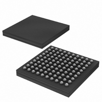
DS3170+ Maxim Integrated Products, DS3170+ Datasheet - Page 103

DS3170+
Manufacturer Part Number
DS3170+
Description
IC TXRX DS3/E3 100-CSBGA
Manufacturer
Maxim Integrated Products
Datasheet
1.DS3170.pdf
(230 pages)
Specifications of DS3170+
Function
Single-Chip Transceiver
Interface
DS3, E3
Number Of Circuits
1
Voltage - Supply
3.135 V ~ 3.465 V
Current - Supply
120mA
Operating Temperature
0°C ~ 70°C
Mounting Type
Surface Mount
Package / Case
100-LBGA
Includes
DS3 Framers, E3 Framers, HDLC Controller, On-Chip BERTs
Lead Free Status / RoHS Status
Lead free / RoHS Compliant
Power (watts)
-
- Current page: 103 of 230
- Download datasheet (3Mb)
The transmit direction inputs codewords from the microprocessor via the register interface and stores the
codewords. It removes the codewords and performs FEAC processing. See
FEAC Controller in the block diagram
Figure 10-22. FEAC Controller Block Diagram
10.9.2 Features
•
•
•
•
10.9.3 Functional Description
The bits in a code are received MSB first, LSB last. When they are output serially, they are output MSB first, LSB
last. The bits in a code in an incoming signal are numbered in the order they are received, 1 (MSB) to 6 (LSB).
However, when a code is stored in a register, the MSB is stored in the lowest numbered bit (0), and the LSB is
stored in the highest numbered bit (5). This is to differentiate between a code in a register and the corresponding
code in a signal.
10.9.3.1 Transmit Data Storage
The Transmit Data Storage block contains the registers for two FEAC codes (C{1:6]) and controller circuitry for
reading and writing the memory. The Transmit Data Storage receives data from the microprocessor interface, and
stores the data in memory. The Transmit FEAC Processor reads the data from the Transmit Data Storage.
10.9.3.2 Transmit FEAC Processor
The Transmit FEAC Processor accepts data from the Transmit Data Storage performs FEAC processing. The
FEAC codes are read from Transmit Data Storage with the MSB (C[1]) in TFCA[0] or TFCB[0], and the LSB (C[6])
in TFCA[5] or TFCB[5].
FEAC processing has four modes of operation (Idle, single code, dual code, and continuous code). In Idle mode, all
ones are output on the outgoing FEAC data stream. In single code mode, the code from TFCA[5:0] is inserted into
a codeword
output. In dual code mode, the code from TFCA[5:0] is inserted into a codeword, and sent ten consecutive times.
Then the code from TFCB[5:0] is inserted into a codeword, and sent ten consecutive times. Once both codewords
Clock Rate
Programmable dual codeword output – The transmit side can be programmed to output a single codeword
ten times, one codeword ten times followed by a second codeword ten times, or a single codeword
continuously.
Four codeword receive FIFO
Fully independent transmit and receive paths
Fully independent Line side and register side timing – The FIFO can be read from or written to at the
register interface side while all line side clocks and signals are inactive, and read from or written to at the line
side while all register interface side clocks and signals are inactive.
Receive
Transmit
DS3/E3
DS3/E3
Adapter
LIU
LIU
(Figure
10-23), and sent ten consecutive times. Once the ten codewords have been sent, all ones are
Encoder
Decoder
B3ZS/
B3ZS/
HDB3
HDB3
TUA1
TAIS
IEEE P1149.1
JTAG Test
Access Port
FEAC
DS3 / E3
Framer
DS3 / E3
Transmit
Receive
Formatter
Buffer
Trace
Trail
HDLC
103 of 230
GEN
UA1
DS3170 DS3/E3 Single-Chip Transceiver
RX BERT
TX BERT
Figure 10-22
Microprocessor
Interface
for the location of the
Related parts for DS3170+
Image
Part Number
Description
Manufacturer
Datasheet
Request
R

Part Number:
Description:
MAX7528KCWPMaxim Integrated Products [CMOS Dual 8-Bit Buffered Multiplying DACs]
Manufacturer:
Maxim Integrated Products
Datasheet:

Part Number:
Description:
Single +5V, fully integrated, 1.25Gbps laser diode driver.
Manufacturer:
Maxim Integrated Products
Datasheet:

Part Number:
Description:
Single +5V, fully integrated, 155Mbps laser diode driver.
Manufacturer:
Maxim Integrated Products
Datasheet:

Part Number:
Description:
VRD11/VRD10, K8 Rev F 2/3/4-Phase PWM Controllers with Integrated Dual MOSFET Drivers
Manufacturer:
Maxim Integrated Products
Datasheet:

Part Number:
Description:
Highly Integrated Level 2 SMBus Battery Chargers
Manufacturer:
Maxim Integrated Products
Datasheet:

Part Number:
Description:
Current Monitor and Accumulator with Integrated Sense Resistor; ; Temperature Range: -40°C to +85°C
Manufacturer:
Maxim Integrated Products

Part Number:
Description:
TSSOP 14/A�/RS-485 Transceivers with Integrated 100O/120O Termination Resis
Manufacturer:
Maxim Integrated Products

Part Number:
Description:
TSSOP 14/A�/RS-485 Transceivers with Integrated 100O/120O Termination Resis
Manufacturer:
Maxim Integrated Products

Part Number:
Description:
QFN 16/A�/AC-DC and DC-DC Peak-Current-Mode Converters with Integrated Step
Manufacturer:
Maxim Integrated Products

Part Number:
Description:
TDFN/A/65V, 1A, 600KHZ, SYNCHRONOUS STEP-DOWN REGULATOR WITH INTEGRATED SWI
Manufacturer:
Maxim Integrated Products

Part Number:
Description:
Integrated Temperature Controller f
Manufacturer:
Maxim Integrated Products

Part Number:
Description:
SOT23-6/I�/45MHz to 650MHz, Integrated IF VCOs with Differential Output
Manufacturer:
Maxim Integrated Products

Part Number:
Description:
SOT23-6/I�/45MHz to 650MHz, Integrated IF VCOs with Differential Output
Manufacturer:
Maxim Integrated Products

Part Number:
Description:
EVALUATION KIT/2.4GHZ TO 2.5GHZ 802.11G/B RF TRANSCEIVER WITH INTEGRATED PA
Manufacturer:
Maxim Integrated Products

Part Number:
Description:
QFN/E/DUAL PCIE/SATA HIGH SPEED SWITCH WITH INTEGRATED BIAS RESISTOR
Manufacturer:
Maxim Integrated Products
Datasheet:


