DS3170+ Maxim Integrated Products, DS3170+ Datasheet - Page 128
DS3170+
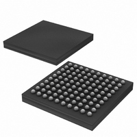
Manufacturer Part Number
DS3170+
Description
IC TXRX DS3/E3 100-CSBGA
Manufacturer
Maxim Integrated Products
Datasheet
1.DS3170.pdf
(230 pages)
Specifications of DS3170+
Function
Single-Chip Transceiver
Interface
DS3, E3
Number Of Circuits
1
Voltage - Supply
3.135 V ~ 3.465 V
Current - Supply
120mA
Operating Temperature
0°C ~ 70°C
Mounting Type
Surface Mount
Package / Case
100-LBGA
Includes
DS3 Framers, E3 Framers, HDLC Controller, On-Chip BERTs
Lead Free Status / RoHS Status
Lead free / RoHS Compliant
Power (watts)
-


Register Name:
Register Description:
Register Address:
Bit #
Name
Default
Bit #
Name
Default
Bits 11 to 10: Global 8KHz Reference Source [1:0] (G8KRS[1:0]). These bits determine the source for the
internally generated 8 kHz reference as well as the internal one second reference, which is derived from the Global
8 kHz reference. The source is selected from the CLAD clock or from the port 8KREF clock source. See
10-12. Global 8 kHz Reference Source Table
These bits are ignored when the G8KIS bit = 1.
Table 10-12. Global 8 kHz Reference Source Table
Bit 9: Global 8KHz Reference Output Select (G8KOS). This bit determines whether GPIO2 pin is used for the
global 8KREFO output signal, or is used as specified by GL.GIOCR.GPIO2S[1:0].
Bit 8: Global 8KHz Reference Input Select (G8KIS). This bit determines whether GPIO4 pin is used for the global
8KREFI input signal, or is used as specified by GL.GIOCR.GPIO4S[1:0]. G8KREFI signal will be low if not
selected. Global 8KREF pin signal will be low if not selected.
Bits 3 to 1: CLAD IO Mode [2:0] (CLAD[2:0]). These bits control the CLAD. See
Table 10-11. CLAD Clock Source Settings
GL.CR2.
G8KIS
CLAD[2:0]
0
0
0
0
1
11X
000
001
010
011
100
101
0 = GPIO2 pin mode selected by
1 = GPIO2 is the global 8KREFO output signal selected by
0 = GPIO4 pin mode selected by
1 = GPIO4 is the global 8KREFI input signal for one second timer and port to use
G8KRS[1:0]
GL.CR2.
15
--
--
0
7
0
XX
00
01
10
11
REFCLK (INPUT)
44.736 MHz
34.368 MHz
51.84 MHz
19.44 MHz
Undefined
Undefined
77.76 MHz
None, the 8KHZ divider is disabled.
Derived from CLAD output clock
8KREF source selected by P8KRS[1:0]
Undefined
GPIO4
14
--
--
0
6
0
GL.CR2
Global Control Register 2
004h
13
GL.GIOCR.
GL.GIOCR.
--
0
5
--
0
SOURCE
128 of 230
GPIO2S[1:0]
GPIO4S[1:0]
12
--
--
0
4
0
G8KRS1
CLAD2
GL.CR2.8KRS[2:0]
11
0
3
0
DS3170 DS3/E3 Single-Chip Transceiver
G8KRS0
CLAD1
10
0
2
0
Table
10-11.
G8K0S
CLAD0
9
0
1
0
G8KIS
--
8
0
0
0
Table
Related parts for DS3170+
Image
Part Number
Description
Manufacturer
Datasheet
Request
R

Part Number:
Description:
MAX7528KCWPMaxim Integrated Products [CMOS Dual 8-Bit Buffered Multiplying DACs]
Manufacturer:
Maxim Integrated Products
Datasheet:
Part Number:
Description:
Single +5V, fully integrated, 1.25Gbps laser diode driver.
Manufacturer:
Maxim Integrated Products
Datasheet:
Part Number:
Description:
Single +5V, fully integrated, 155Mbps laser diode driver.
Manufacturer:
Maxim Integrated Products
Datasheet:
Part Number:
Description:
VRD11/VRD10, K8 Rev F 2/3/4-Phase PWM Controllers with Integrated Dual MOSFET Drivers
Manufacturer:
Maxim Integrated Products
Datasheet:
Part Number:
Description:
Highly Integrated Level 2 SMBus Battery Chargers
Manufacturer:
Maxim Integrated Products
Datasheet:
Part Number:
Description:
Current Monitor and Accumulator with Integrated Sense Resistor; ; Temperature Range: -40°C to +85°C
Manufacturer:
Maxim Integrated Products
Part Number:
Description:
TSSOP 14/A�/RS-485 Transceivers with Integrated 100O/120O Termination Resis
Manufacturer:
Maxim Integrated Products
Part Number:
Description:
TSSOP 14/A�/RS-485 Transceivers with Integrated 100O/120O Termination Resis
Manufacturer:
Maxim Integrated Products
Part Number:
Description:
QFN 16/A�/AC-DC and DC-DC Peak-Current-Mode Converters with Integrated Step
Manufacturer:
Maxim Integrated Products
Part Number:
Description:
TDFN/A/65V, 1A, 600KHZ, SYNCHRONOUS STEP-DOWN REGULATOR WITH INTEGRATED SWI
Manufacturer:
Maxim Integrated Products
Part Number:
Description:
Integrated Temperature Controller f
Manufacturer:
Maxim Integrated Products
Part Number:
Description:
SOT23-6/I�/45MHz to 650MHz, Integrated IF VCOs with Differential Output
Manufacturer:
Maxim Integrated Products
Part Number:
Description:
SOT23-6/I�/45MHz to 650MHz, Integrated IF VCOs with Differential Output
Manufacturer:
Maxim Integrated Products
Part Number:
Description:
EVALUATION KIT/2.4GHZ TO 2.5GHZ 802.11G/B RF TRANSCEIVER WITH INTEGRATED PA
Manufacturer:
Maxim Integrated Products
Part Number:
Description:
QFN/E/DUAL PCIE/SATA HIGH SPEED SWITCH WITH INTEGRATED BIAS RESISTOR
Manufacturer:
Maxim Integrated Products
Datasheet: