DS3170+ Maxim Integrated Products, DS3170+ Datasheet - Page 157
DS3170+
Manufacturer Part Number
DS3170+
Description
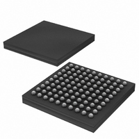
IC TXRX DS3/E3 100-CSBGA
Manufacturer
Maxim Integrated Products
Datasheet
1.DS3170.pdf
(230 pages)
Specifications of DS3170+
Function
Single-Chip Transceiver
Interface
DS3, E3
Number Of Circuits
1
Voltage - Supply
3.135 V ~ 3.465 V
Current - Supply
120mA
Operating Temperature
0°C ~ 70°C
Mounting Type
Surface Mount
Package / Case
100-LBGA
Includes
DS3 Framers, E3 Framers, HDLC Controller, On-Chip BERTs
Lead Free Status / RoHS Status
Lead free / RoHS Compliant
Power (watts)
-


Bit 1: Transmit FCS Processing Disable (TFPD) – This bit controls whether or not an FCS is calculated and
appended to the end of each packet. When 0, the calculated FCS bytes are appended to the end of the packet.
When 1, the packet is transmitted without an FCS.
Bit 0: Transmit FIFO Reset (TFRST) – When 0, the Transmit FIFO will resume normal operations, however, data
is discarded until a start of packet is received after RAM power-up is completed. When 1, the Transmit FIFO is
emptied, any transfer in progress is halted, the FIFO RAM is powered down, and all incoming data is discarded (all
TFDR register writes are ignored).
Register Name:
Register Description:
Register Address:
Bit #
Name
Default
Bit #
Name
Default
Note: The FIFO data and status are loaded into the Transmit FIFO when the Transmit FIFO Data (TFD[7:0]) is
written (upper byte write). When read, the value of these bits is always zero.
Bits 15 to 8: Transmit FIFO Data (TFD[7:0]) – These eight bits are the packet data to be stored in the Transmit
FIFO. TFD[7] is the MSB, and TFD[0] is the LSB. If bit reordering is disabled, TFD[0] is the first bit transmitted, and
TFD[7] is the last bit transmitted. If bit reordering is enabled, TFD[7] is the first bit transmitted, and TFD[0] is the
last bit transmitted.
Bit 0: Transmit FIFO Data Packet End (TDPE) – When 0, the Transmit FIFO data is not a packet end. When 1,
the Transmit FIFO data is a packet end.
Register Name:
Register Description:
Register Address:
Bit #
Name
Bit #
Name
Bits 13 to 8: Transmit FIFO Fill Level (TFFL[5:0]) – These six bits indicate the number of eight byte groups
available for storage (do not contain data) in the Transmit FIFO. E.g., a value of 21 (15h) indicates the FIFO has
168 (A8h) to 175 (AFh) bytes are available for storage.
Bit 2: Transmit FIFO Full (TFF) – When 0, the Transmit FIFO contains 255 or less bytes of data. When 1, the
Transmit FIFO is full.
Bit 1: Transmit FIFO Empty (TFE) – When 0, the Transmit FIFO contains at least one byte of data. When 1, the
Transmit FIFO is empty.
Bit 0: Transmit HDLC Data Storage Available (THDA) – When 0, the Transmit FIFO has less storage space
available in the Transmit FIFO than the Transmit HDLC data storage available level (TDAL[4:0]). When 1, the
Transmit FIFO has the same or more storage space available than the Transmit FIFO HDLC data storage available
level.
TFD7
15
15
--
--
--
0
7
0
7
TFD6
14
14
--
--
--
0
6
0
6
HDLC.TFDR
HDLC Transmit FIFO Data Register
0A2h
HDLC.TSR
HDLC Transmit Status Register
0A4h
TFFL5
TFD5
13
13
--
--
0
5
0
5
157 of 230
TFFL4
TFD4
12
12
--
--
0
4
0
4
TFFL3
TFD3
11
11
--
--
0
3
0
3
DS3170 DS3/E3 Single-Chip Transceiver
TFFL2
TFD2
TFF
10
10
--
0
2
0
2
TFFL1
TFD1
TFE
--
9
0
1
0
9
1
THDA
TFFL0
TDPE
TFD0
8
0
0
0
8
0
Related parts for DS3170+
Image
Part Number
Description
Manufacturer
Datasheet
Request
R

Part Number:
Description:
MAX7528KCWPMaxim Integrated Products [CMOS Dual 8-Bit Buffered Multiplying DACs]
Manufacturer:
Maxim Integrated Products
Datasheet:
Part Number:
Description:
Single +5V, fully integrated, 1.25Gbps laser diode driver.
Manufacturer:
Maxim Integrated Products
Datasheet:
Part Number:
Description:
Single +5V, fully integrated, 155Mbps laser diode driver.
Manufacturer:
Maxim Integrated Products
Datasheet:
Part Number:
Description:
VRD11/VRD10, K8 Rev F 2/3/4-Phase PWM Controllers with Integrated Dual MOSFET Drivers
Manufacturer:
Maxim Integrated Products
Datasheet:
Part Number:
Description:
Highly Integrated Level 2 SMBus Battery Chargers
Manufacturer:
Maxim Integrated Products
Datasheet:
Part Number:
Description:
Current Monitor and Accumulator with Integrated Sense Resistor; ; Temperature Range: -40°C to +85°C
Manufacturer:
Maxim Integrated Products
Part Number:
Description:
TSSOP 14/A�/RS-485 Transceivers with Integrated 100O/120O Termination Resis
Manufacturer:
Maxim Integrated Products
Part Number:
Description:
TSSOP 14/A�/RS-485 Transceivers with Integrated 100O/120O Termination Resis
Manufacturer:
Maxim Integrated Products
Part Number:
Description:
QFN 16/A�/AC-DC and DC-DC Peak-Current-Mode Converters with Integrated Step
Manufacturer:
Maxim Integrated Products
Part Number:
Description:
TDFN/A/65V, 1A, 600KHZ, SYNCHRONOUS STEP-DOWN REGULATOR WITH INTEGRATED SWI
Manufacturer:
Maxim Integrated Products
Part Number:
Description:
Integrated Temperature Controller f
Manufacturer:
Maxim Integrated Products
Part Number:
Description:
SOT23-6/I�/45MHz to 650MHz, Integrated IF VCOs with Differential Output
Manufacturer:
Maxim Integrated Products
Part Number:
Description:
SOT23-6/I�/45MHz to 650MHz, Integrated IF VCOs with Differential Output
Manufacturer:
Maxim Integrated Products
Part Number:
Description:
EVALUATION KIT/2.4GHZ TO 2.5GHZ 802.11G/B RF TRANSCEIVER WITH INTEGRATED PA
Manufacturer:
Maxim Integrated Products
Part Number:
Description:
QFN/E/DUAL PCIE/SATA HIGH SPEED SWITCH WITH INTEGRATED BIAS RESISTOR
Manufacturer:
Maxim Integrated Products
Datasheet: