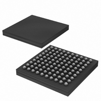
DS3170+ Maxim Integrated Products, DS3170+ Datasheet - Page 145

DS3170+
Manufacturer Part Number
DS3170+
Description
IC TXRX DS3/E3 100-CSBGA
Manufacturer
Maxim Integrated Products
Datasheet
1.DS3170.pdf
(230 pages)
Specifications of DS3170+
Function
Single-Chip Transceiver
Interface
DS3, E3
Number Of Circuits
1
Voltage - Supply
3.135 V ~ 3.465 V
Current - Supply
120mA
Operating Temperature
0°C ~ 70°C
Mounting Type
Surface Mount
Package / Case
100-LBGA
Includes
DS3 Framers, E3 Framers, HDLC Controller, On-Chip BERTs
Lead Free Status / RoHS Status
Lead free / RoHS Compliant
Power (watts)
-
- Current page: 145 of 230
- Download datasheet (3Mb)
must be changed to zero and back to one for another pattern to be loaded. Loading a new pattern will forces the
receive pattern generator out of the “Sync” state which causes a resynchronization to be initiated. Note: QRSS,
PTS, PLF[4:0}, PTF[4:0], and BSP[31:0] must not change from the time this bit transitions from 0 to 1 until four
receive clock cycles after this bit transitions from 0 to 1.
Bit 4: Receive Pattern Inversion Control (RPIC) – When 0, the receive incoming data stream is not altered.
When 1, the receive incoming data stream is inverted.
Bit 3: Manual Pattern Resynchronization (MPR) – A zero to one transition of this bit will cause the receive
pattern generator to resynchronize to the incoming pattern. This bit must be changed to zero and back to one for
another resynchronization to be initiated. Note: A manual resynchronization forces the receive pattern generator
out of the “Sync” state.
Bit 2: Automatic Pattern Resynchronization Disable (APRD) – When 0, the receive pattern generator will
automatically resynchronize to the incoming pattern if six or more times during the current 64-bit window the
incoming data stream bit and the receive pattern generator output bit did not match. When 1, the receive pattern
generator will not automatically resynchronize to the incoming pattern.
Bit 1: Transmit New Pattern Load (TNPL) – A zero to one transition of this bit will cause the programmed test
pattern (QRSS, PTS, PLF[4:0}, PTF[4:0], and BSP[31:0]) to be loaded in to the transmit pattern generator. This bit
must be changed to zero and back to one for another pattern to be loaded. Note: QRSS, PTS, PLF[4:0}, PTF[4:0],
and BSP[31:0] must not change from the time this bit transitions from 0 to 1 until four transmit clock cycles after this
bit transitions from 0 to 1.
Bit 0: Transmit Pattern Inversion Control (TPIC) – When 0, the transmit outgoing data stream is not altered.
When 1, the transmit outgoing data stream is inverted.
Register Name:
Register Description:
Register Address:
Bit #
Name
Default
Bit #
Name
Default
Bits 12 to 8: Pattern Tap Feedback (PTF[4:0]) – These five bits control the PRBS “tap” feedback of the pattern
generator. The “tap” feedback will be from bit y of the pattern generator (y = PTF[4:0] +1). These bits are ignored
when programmed for a repetitive pattern. For a PRBS signal, the feedback is an XOR of bit n and bit y.
Bit 6: QRSS Enable (QRSS) – When 0, the pattern generator configuration is controlled by PTS, PLF[4:0], and
PTF[4:0], and BSP[31:0]. When 1, the pattern generator configuration is forced to a PRBS pattern with a
generating polynomial of x
output bits are all zero.
Bit 5: Pattern Type Select (PTS) – When 0, the pattern is a PRBS pattern. When 1, the pattern is a repetitive
pattern.
Bits 4 to 0: Pattern Length Feedback (PLF[4:0]) – These five bits control the “length” feedback of the pattern
generator. The “length” feedback will be from bit n of the pattern generator (n = PLF[4:0] +1). For a PRBS signal,
the feedback is an XOR of bit n and bit y. For a repetitive pattern the feedback is bit n.
15
--
--
0
7
0
QRSS
20
14
--
+ x
0
6
0
17
BERT.PCR
BERT Pattern Configuration Register
062h
+ 1. The output of the pattern generator will be forced to one if the next fourteen
PTS
13
--
0
5
0
145 of 230
PTF4
PLF4
12
0
4
0
PTF3
PLF3
11
0
3
0
DS3170 DS3/E3 Single-Chip Transceiver
PTF2
PLF2
10
0
2
0
PTF1
PLF1
9
0
1
0
PTF0
PLF0
8
0
0
0
Related parts for DS3170+
Image
Part Number
Description
Manufacturer
Datasheet
Request
R

Part Number:
Description:
MAX7528KCWPMaxim Integrated Products [CMOS Dual 8-Bit Buffered Multiplying DACs]
Manufacturer:
Maxim Integrated Products
Datasheet:

Part Number:
Description:
Single +5V, fully integrated, 1.25Gbps laser diode driver.
Manufacturer:
Maxim Integrated Products
Datasheet:

Part Number:
Description:
Single +5V, fully integrated, 155Mbps laser diode driver.
Manufacturer:
Maxim Integrated Products
Datasheet:

Part Number:
Description:
VRD11/VRD10, K8 Rev F 2/3/4-Phase PWM Controllers with Integrated Dual MOSFET Drivers
Manufacturer:
Maxim Integrated Products
Datasheet:

Part Number:
Description:
Highly Integrated Level 2 SMBus Battery Chargers
Manufacturer:
Maxim Integrated Products
Datasheet:

Part Number:
Description:
Current Monitor and Accumulator with Integrated Sense Resistor; ; Temperature Range: -40°C to +85°C
Manufacturer:
Maxim Integrated Products

Part Number:
Description:
TSSOP 14/A�/RS-485 Transceivers with Integrated 100O/120O Termination Resis
Manufacturer:
Maxim Integrated Products

Part Number:
Description:
TSSOP 14/A�/RS-485 Transceivers with Integrated 100O/120O Termination Resis
Manufacturer:
Maxim Integrated Products

Part Number:
Description:
QFN 16/A�/AC-DC and DC-DC Peak-Current-Mode Converters with Integrated Step
Manufacturer:
Maxim Integrated Products

Part Number:
Description:
TDFN/A/65V, 1A, 600KHZ, SYNCHRONOUS STEP-DOWN REGULATOR WITH INTEGRATED SWI
Manufacturer:
Maxim Integrated Products

Part Number:
Description:
Integrated Temperature Controller f
Manufacturer:
Maxim Integrated Products

Part Number:
Description:
SOT23-6/I�/45MHz to 650MHz, Integrated IF VCOs with Differential Output
Manufacturer:
Maxim Integrated Products

Part Number:
Description:
SOT23-6/I�/45MHz to 650MHz, Integrated IF VCOs with Differential Output
Manufacturer:
Maxim Integrated Products

Part Number:
Description:
EVALUATION KIT/2.4GHZ TO 2.5GHZ 802.11G/B RF TRANSCEIVER WITH INTEGRATED PA
Manufacturer:
Maxim Integrated Products

Part Number:
Description:
QFN/E/DUAL PCIE/SATA HIGH SPEED SWITCH WITH INTEGRATED BIAS RESISTOR
Manufacturer:
Maxim Integrated Products
Datasheet:


