DS3170+ Maxim Integrated Products, DS3170+ Datasheet - Page 65
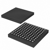
DS3170+
Manufacturer Part Number
DS3170+
Description
IC TXRX DS3/E3 100-CSBGA
Manufacturer
Maxim Integrated Products
Datasheet
1.DS3170.pdf
(230 pages)
Specifications of DS3170+
Function
Single-Chip Transceiver
Interface
DS3, E3
Number Of Circuits
1
Voltage - Supply
3.135 V ~ 3.465 V
Current - Supply
120mA
Operating Temperature
0°C ~ 70°C
Mounting Type
Surface Mount
Package / Case
100-LBGA
Includes
DS3 Framers, E3 Framers, HDLC Controller, On-Chip BERTs
Lead Free Status / RoHS Status
Lead free / RoHS Compliant
Power (watts)
-


Table 10-10. Reset and Power-Down Sources
Register Bit States—F0: Forced to 0; F1: Forced to 1; 0: Set to 0; 1: Set to 1; X: Don’t care
Forced: Internally controlled; Set: User controlled
The reset signals in the device are asynchronous so they no not require a clock to put the logic into the reset state.
Clock signals may be needed to make the logic come out of the reset state.
The power-down function disables the appropriate clocks to cause the logic to generate a minimum of power. It
also puts the LIU circuits into the power-down mode. The 8KREF and ONESEC circuits can be powered down by
disabling the 8KREF source. The CLAD can also be powered down by disabling it.
After a global reset, all of the control and status registers are set to their default values and all the other flops are
reset to their reset values. The global register GL.CR1.RSTDP, and the port register PORT.CR1.RSTDP and
PORT.CR1.PD bits, are set after the global reset. A valid initialization sequence would be to clear the
PORT.CR1.PD bit, write to all of the configuration registers to set them in the desired modes, then clear the
GL.CR1.RSTDP and PORT.CR1.RSTDP bits. This would cause the logic in the port to start up in a repeatable
sequence. The device can also be initialized by clearing the GL.CR1.RSTDP, PORT.CR1.RSTDP and
PORT.CR1.PD them writing to all of the configuration registers to set them in the desired modes, and clearing all of
the latched status bits. The second initialization scheme could cause the device to temporarily go into modes of
operation that were not requested, but will quickly go into the requested modes of operation.
Some of the IO pins are put in a known state at reset. The transmit LIU outputs TXP and TXN are quiet and will not
drive positive or negative pulses. The global IO pins (GPIO[7:0]) are set as inputs at global reset. The port output
pins (TLCLK, TPOS/TDAT, TNEG, TOHCLK, TOHSOF, TSOFO/TDEN, TCLKO/TGCLK, ROH, ROHCLK,
ROHSOF, RSER, RSOFO/RDEN, RCLKO/RGCLK) are driven low at global or port reset and should stay low until
after the port power-down PORT.CR1.PD and port data path reset PORT.CR1.RSTDP bits are cleared. The
processor port three-state output pins (D[15:0], RDY, INT) are forced into the high impedance state when the RST
pin is active, but not when the GL.CR1.RST bit is active.
After reset, the device will be in the default configuration:: The latched status bits are enabled to be cleared on
write. The CLAD is disabled. The global 8KREF and one-second timers are disabled. The line interface is in B3ZS
mode and the LIU is disabled and the transmit line pins are also disabled. The frame mode is DS3 C-bit with
automatic downstream AIS on LOS or OOF is enabled and automatic RDI on LOF, LOS, SEF or AIS is enabled
and automatic FEBE is enabled. Transmit clock comes from the REFCLK pin. The pin inversion on all pins is
disabled.
Individual blocks are reset and powered down when not used determined by the settings in the line mode bits
PORT.CR2.LM[2:0] and framer mode bits PORT.CR2.FM[2:0].
PIN
0
1
1
1
1
1
1
1
1
1
F0
1
0
0
0
0
0
0
0
0
F1
F1
1
1
1
0
0
0
0
0
REGISTER BITS
F0
F0
1
0
0
1
0
0
0
0
F1
F1
F1
F1
X
X
1
1
0
0
F1
F1
F1
F1
1
0
1
0
1
0
1
1
0
0
0
0
0
0
0
0
65 of 230
INTERNAL SIGNALS
1
1
1
1
1
0
0
0
0
0
1
1
1
0
0
1
0
0
0
0
1
1
1
1
1
1
1
1
1
0
DS3170 DS3/E3 Single-Chip Transceiver
1
1
1
1
0
1
1
0
1
0
Related parts for DS3170+
Image
Part Number
Description
Manufacturer
Datasheet
Request
R

Part Number:
Description:
MAX7528KCWPMaxim Integrated Products [CMOS Dual 8-Bit Buffered Multiplying DACs]
Manufacturer:
Maxim Integrated Products
Datasheet:
Part Number:
Description:
Single +5V, fully integrated, 1.25Gbps laser diode driver.
Manufacturer:
Maxim Integrated Products
Datasheet:
Part Number:
Description:
Single +5V, fully integrated, 155Mbps laser diode driver.
Manufacturer:
Maxim Integrated Products
Datasheet:
Part Number:
Description:
VRD11/VRD10, K8 Rev F 2/3/4-Phase PWM Controllers with Integrated Dual MOSFET Drivers
Manufacturer:
Maxim Integrated Products
Datasheet:
Part Number:
Description:
Highly Integrated Level 2 SMBus Battery Chargers
Manufacturer:
Maxim Integrated Products
Datasheet:
Part Number:
Description:
Current Monitor and Accumulator with Integrated Sense Resistor; ; Temperature Range: -40°C to +85°C
Manufacturer:
Maxim Integrated Products
Part Number:
Description:
TSSOP 14/A�/RS-485 Transceivers with Integrated 100O/120O Termination Resis
Manufacturer:
Maxim Integrated Products
Part Number:
Description:
TSSOP 14/A�/RS-485 Transceivers with Integrated 100O/120O Termination Resis
Manufacturer:
Maxim Integrated Products
Part Number:
Description:
QFN 16/A�/AC-DC and DC-DC Peak-Current-Mode Converters with Integrated Step
Manufacturer:
Maxim Integrated Products
Part Number:
Description:
TDFN/A/65V, 1A, 600KHZ, SYNCHRONOUS STEP-DOWN REGULATOR WITH INTEGRATED SWI
Manufacturer:
Maxim Integrated Products
Part Number:
Description:
Integrated Temperature Controller f
Manufacturer:
Maxim Integrated Products
Part Number:
Description:
SOT23-6/I�/45MHz to 650MHz, Integrated IF VCOs with Differential Output
Manufacturer:
Maxim Integrated Products
Part Number:
Description:
SOT23-6/I�/45MHz to 650MHz, Integrated IF VCOs with Differential Output
Manufacturer:
Maxim Integrated Products
Part Number:
Description:
EVALUATION KIT/2.4GHZ TO 2.5GHZ 802.11G/B RF TRANSCEIVER WITH INTEGRATED PA
Manufacturer:
Maxim Integrated Products
Part Number:
Description:
QFN/E/DUAL PCIE/SATA HIGH SPEED SWITCH WITH INTEGRATED BIAS RESISTOR
Manufacturer:
Maxim Integrated Products
Datasheet: