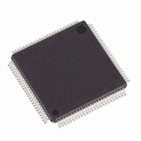
DS21552L+ Maxim Integrated Products, DS21552L+ Datasheet - Page 76

DS21552L+
Manufacturer Part Number
DS21552L+
Description
IC TXRX T1 1-CHIP 5V 100-LQFP
Manufacturer
Maxim Integrated Products
Datasheet
1.DS21352L.pdf
(137 pages)
Specifications of DS21552L+
Function
Single-Chip Transceiver
Interface
E1, HDLC, J1, T1
Number Of Circuits
1
Voltage - Supply
4.75 V ~ 5.25 V
Current - Supply
75mA
Operating Temperature
0°C ~ 70°C
Mounting Type
Surface Mount
Package / Case
100-LQFP
Includes
DSX-1 and CSU Line Build-Out Generator, HDLC Controller, In-Band Loop Code Generator and Detector
Product
Framer
Number Of Transceivers
1
Data Rate
64 Kbps
Supply Voltage (max)
3.465 V
Supply Voltage (min)
3.135 V
Supply Current (max)
75 mA (Typ)
Maximum Operating Temperature
+ 70 C
Minimum Operating Temperature
0 C
Mounting Style
SMD/SMT
Ic Interface Type
Parallel, Serial
Supply Voltage Range
4.75V To 5.25V
Operating Temperature Range
0°C To +70°C
Digital Ic Case Style
LQFP
No. Of Pins
100
Filter Terminals
SMD
Rohs Compliant
Yes
Lead Free Status / RoHS Status
Lead free / RoHS Compliant
Power (watts)
-
Lead Free Status / Rohs Status
Lead free / RoHS Compliant
- Current page: 76 of 137
- Download datasheet (2Mb)
THFR: TRANSMIT HDLC FIFO (Address=08 Hex)
RDC1: RECEIVE HDLC DS0 CONTROL REGISTER 1 (Address=90 Hex)
SYMBOL
SYMBOL
THFR7
RDS0E
(MSB)
(MSB)
RDS0M
THFR7
THFR6
THFR5
THFR4
THFR3
THFR2
THFR1
THFR0
RDS0E
BOC5
BOC4
BOC3
BOC2
BOC1
BOC0
RD4
RD3
RD2
-
THFR6
POSITION
POSITION
TBOC.5
TBOC.4
TBOC.3
TBOC.2
TBOC.1
TBOC.0
THFR.7
THFR.6
THFR.5
THFR.4
THFR.3
THFR.2
THFR.1
THFR.0
RDC1.7
RDC1.6
RDC1.5
RDC1.4
RDC1.3
RDC1.2
-
RDS0M
THFR5
0 = source FDL data from the TLINK pin
1 = source FDL data from the onboard HDLC and BOC controller
BOC Bit 5. Last bit transmitted of the 6–bit codeword.
BOC Bit 4.
BOC Bit 3.
BOC Bit 2.
BOC Bit 1.
BOC Bit 0. First bit transmitted of the 6–bit codeword.
NAME AND DESCRIPTION
HDLC Data Bit 7. MSB of a HDLC packet data byte.
HDLC Data Bit 6.
HDLC Data Bit 5.
HDLC Data Bit 4.
HDLC Data Bit 3.
HDLC Data Bit 2.
HDLC Data Bit 1.
HDLC Data Bit 0. LSB of a HDLC packet data byte.
NAME AND DESCRIPTION
HDLC DS0 Enable.
0 = use the receive HDLC controller for the FDL.
1 = use the receive HDLC controller for one or more DS0 channels.
Not Assigned. Should be set to 0.
DS0 Selection Mode.
0 = utilize the RD0 to RD4 bits to select which single DS0 channel to use.
1 = utilize the RCHBLK control registers to select which DS0 channels to use.
DS0 Channel Select Bit 4. MSB of the DS0 channel select.
DS0 Channel Select Bit 3.
DS0 Channel Select Bit 2.
THFR4
RD4
76 of 137
THFR3
RD3
THFR2
RD2
THFR1
RD1
THFR0
(LSB)
(LSB)
RD0
Related parts for DS21552L+
Image
Part Number
Description
Manufacturer
Datasheet
Request
R

Part Number:
Description:
Manufacturer:
Maxim Integrated Products
Datasheet:

Part Number:
Description:
Ds2155 T1/e1/j1 Single-chip Transceiver
Manufacturer:
Maxim Integrated Products, Inc.
Datasheet:

Part Number:
Description:
MAX7528KCWPMaxim Integrated Products [CMOS Dual 8-Bit Buffered Multiplying DACs]
Manufacturer:
Maxim Integrated Products
Datasheet:

Part Number:
Description:
Single +5V, fully integrated, 1.25Gbps laser diode driver.
Manufacturer:
Maxim Integrated Products
Datasheet:

Part Number:
Description:
Single +5V, fully integrated, 155Mbps laser diode driver.
Manufacturer:
Maxim Integrated Products
Datasheet:

Part Number:
Description:
VRD11/VRD10, K8 Rev F 2/3/4-Phase PWM Controllers with Integrated Dual MOSFET Drivers
Manufacturer:
Maxim Integrated Products
Datasheet:

Part Number:
Description:
Highly Integrated Level 2 SMBus Battery Chargers
Manufacturer:
Maxim Integrated Products
Datasheet:

Part Number:
Description:
Current Monitor and Accumulator with Integrated Sense Resistor; ; Temperature Range: -40°C to +85°C
Manufacturer:
Maxim Integrated Products

Part Number:
Description:
TSSOP 14/A°/RS-485 Transceivers with Integrated 100O/120O Termination Resis
Manufacturer:
Maxim Integrated Products

Part Number:
Description:
TSSOP 14/A°/RS-485 Transceivers with Integrated 100O/120O Termination Resis
Manufacturer:
Maxim Integrated Products

Part Number:
Description:
QFN 16/A°/AC-DC and DC-DC Peak-Current-Mode Converters with Integrated Step
Manufacturer:
Maxim Integrated Products

Part Number:
Description:
TDFN/A/65V, 1A, 600KHZ, SYNCHRONOUS STEP-DOWN REGULATOR WITH INTEGRATED SWI
Manufacturer:
Maxim Integrated Products

Part Number:
Description:
Integrated Temperature Controller f
Manufacturer:
Maxim Integrated Products

Part Number:
Description:
SOT23-6/I°/45MHz to 650MHz, Integrated IF VCOs with Differential Output
Manufacturer:
Maxim Integrated Products

Part Number:
Description:
SOT23-6/I°/45MHz to 650MHz, Integrated IF VCOs with Differential Output
Manufacturer:
Maxim Integrated Products


