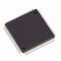
DS21552L+ Maxim Integrated Products, DS21552L+ Datasheet - Page 21

DS21552L+
Manufacturer Part Number
DS21552L+
Description
IC TXRX T1 1-CHIP 5V 100-LQFP
Manufacturer
Maxim Integrated Products
Datasheet
1.DS21352L.pdf
(137 pages)
Specifications of DS21552L+
Function
Single-Chip Transceiver
Interface
E1, HDLC, J1, T1
Number Of Circuits
1
Voltage - Supply
4.75 V ~ 5.25 V
Current - Supply
75mA
Operating Temperature
0°C ~ 70°C
Mounting Type
Surface Mount
Package / Case
100-LQFP
Includes
DSX-1 and CSU Line Build-Out Generator, HDLC Controller, In-Band Loop Code Generator and Detector
Product
Framer
Number Of Transceivers
1
Data Rate
64 Kbps
Supply Voltage (max)
3.465 V
Supply Voltage (min)
3.135 V
Supply Current (max)
75 mA (Typ)
Maximum Operating Temperature
+ 70 C
Minimum Operating Temperature
0 C
Mounting Style
SMD/SMT
Ic Interface Type
Parallel, Serial
Supply Voltage Range
4.75V To 5.25V
Operating Temperature Range
0°C To +70°C
Digital Ic Case Style
LQFP
No. Of Pins
100
Filter Terminals
SMD
Rohs Compliant
Yes
Lead Free Status / RoHS Status
Lead free / RoHS Compliant
Power (watts)
-
Lead Free Status / Rohs Status
Lead free / RoHS Compliant
4.1.3 PARALLEL CONTROL PORT PINS
Signal Name:
Signal Description:
Signal Type:
Flags host controller during conditions and change of conditions defined in the Status Registers 1 and 2 and the HDLC Status
Register. Active low, open drain output
Signal Name:
Signal Description:
Signal Type:
Selects the DS2152 mode when high or the DS21352/552 mode when low. If high, the JTRST is internally pulled low. If low,
JTRST has normal JTAG functionality. This pin has a 10k pull up resistor.
Signal Name:
Signal Description:
Signal Type:
Set high to 3–state all output and I/O pins (including the parallel control port) when FMS = 1 or when FMS = 0 and JTRST* is
tied low. Set low for normal operation. Ignored when FMS = 0 and JTRST* = 1. Useful for board level testing.
Signal Name:
Signal Description:
Signal Type:
Set low to select non–multiplexed bus operation. Set high to select multiplexed bus operation.
Signal Name:
Signal Description:
Signal Type:
In non–multiplexed bus operation (MUX = 0), serves as the data bus. In multiplexed bus operation (MUX = 1), serves as a 8–
bit multiplexed address / data bus.
Signal Name:
Signal Description:
Signal Type:
In non–multiplexed bus operation (MUX = 0), serves as the address bus. In multiplexed bus operation (MUX = 1), these pins
are not used and should be tied low.
Signal Name:
Signal Description:
Signal Type:
Strap high to select Motorola bus timing; strap low to select Intel bus timing. This pin controls the function of the RD*(DS*),
ALE(AS), and WR*(R/W*) pins. If BTS = 1, then these pins assume the function listed in parenthesis ().
Signal Name:
Signal Description:
Signal Type:
RD* and DS* are active low signals. DS active HIGH when MUX = 0. See bus timing diagrams.
INT*
Interrupt
Output
FMS
Framer Mode Select
Input
TEST
3–State Control
Input
MUX
Bus Operation
Input
AD0 TO AD7
Data Bus [D0 to D7] or Address/Data Bus
Input
A0 TO A6
Address Bus
Input
BTS
Bus Type Select
Input
RD*(DS*)
Read Input - Data Strobe
Input
21 of 137


