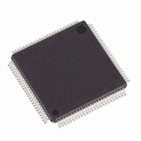
DS21552L+ Maxim Integrated Products, DS21552L+ Datasheet - Page 57

DS21552L+
Manufacturer Part Number
DS21552L+
Description
IC TXRX T1 1-CHIP 5V 100-LQFP
Manufacturer
Maxim Integrated Products
Datasheet
1.DS21352L.pdf
(137 pages)
Specifications of DS21552L+
Function
Single-Chip Transceiver
Interface
E1, HDLC, J1, T1
Number Of Circuits
1
Voltage - Supply
4.75 V ~ 5.25 V
Current - Supply
75mA
Operating Temperature
0°C ~ 70°C
Mounting Type
Surface Mount
Package / Case
100-LQFP
Includes
DSX-1 and CSU Line Build-Out Generator, HDLC Controller, In-Band Loop Code Generator and Detector
Product
Framer
Number Of Transceivers
1
Data Rate
64 Kbps
Supply Voltage (max)
3.465 V
Supply Voltage (min)
3.135 V
Supply Current (max)
75 mA (Typ)
Maximum Operating Temperature
+ 70 C
Minimum Operating Temperature
0 C
Mounting Style
SMD/SMT
Ic Interface Type
Parallel, Serial
Supply Voltage Range
4.75V To 5.25V
Operating Temperature Range
0°C To +70°C
Digital Ic Case Style
LQFP
No. Of Pins
100
Filter Terminals
SMD
Rohs Compliant
Yes
Lead Free Status / RoHS Status
Lead free / RoHS Compliant
Power (watts)
-
Lead Free Status / Rohs Status
Lead free / RoHS Compliant
RS1 TO RS12: RECEIVE SIGNALING REGISTERS (Address=60 to 6B Hex)
A(8)
A(16)
A(24)
B(8)
B(16)
B(24)
A/C(8)
A/C(16)
A/C(24)
B/D(8)
B/D(16)
B/D(24)
Each Receive Signaling Register (RS1 to RS12) reports the incoming robbed bit signaling from eight
DS0 channels. In the ESF framing mode, there can be up to four signaling bits per channel (A, B, C, and
D). In the D4 framing mode, there are only two signaling bits per channel (A and B). In the D4 framing
mode, the framer will replace the C and D signaling bit positions with the A and B signaling bits from the
previous multiframe. Hence, whether the framer is operated in either framing mode, the user needs only
to retrieve the signaling bits every 3 ms. The bits in the Receive Signaling Registers are updated on
multiframe boundaries so the user can utilize the Receive Multiframe Interrupt in the Receive Status
Register 2 (SR2.7) to know when to retrieve the signaling bits. The Receive Signaling Registers are
frozen and not updated during a loss of sync condition (SR1.0=1). They will contain the most recent
signaling information before the “OOF” occurred. The signaling data reported in RS1 to RS12 is also
available at the RSIG and RSER pins.
A change in the signaling bits from one multiframe to the next will cause the RSC status bit (SR2.0) to be
set. The user can enable the INT pin to toggle low upon detection of a change in signaling by setting the
IMR2.0 bit. Once a signaling change has been detected, the user has at least 2.75 ms to read the data out
of the RS1 to RS12 registers before the data will be lost.
(MSB)
SYMBOL
D(24)
A(1)
A(7)
A(15)
A(23)
B(7)
B(15)
B(23)
A/C(7)
A/C(15)
A/C(23)
B/D(7)
B/D(15)
B/D(23)
POSITION
RS12.7
RS1.0
A(6)
A(14)
A(22)
B(6)
B(14)
B(22)
A/C(6)
A/C(14)
A/C(22)
B/D(6)
B/D(14)
B/D(22)
NAME AND DESCRIPTION
Signaling Bit D in Channel 24
Signaling Bit A in Channel 1
A(5)
A(13)
A(21)
B(5)
B(13)
B(21)
A/C(5)
A/C(13)
A/C(21)
B/D(5)
B/D(13)
B/D(21)
A(4)
A(12)
A(20)
B(4)
B(12)
B(20)
A/C(4)
A/C(12)
A/C(20)
B/D(4)
B/D(12)
B/D(20)
57 of 137
A(3)
A(11)
A(19)
B(3)
B(11)
B(19)
A/C(3)
A/C(11)
A/C(19)
B/D(3)
B/D(11)
B/D(19)
A(2)
A(10)
A(18)
B(2)
B(10)
B(18)
A/C(2)
A/C(10)
A/C(18)
B/D(2)
B/D(10)
B/D(18)
A(1)
A(9)
A(17)
B(1)
B(9)
B(17)
A/C(1)
A/C(9)
A/C(17)
B/D(1)
B/D(9)
B/D(17)
(LSB)
RS1 (60)
RS2 (61)
RS3 (62)
RS4 (63)
RS5 (64)
RS6 (65)
RS7 (66)
RS8 (67)
RS9 (68)
RS10 (69)
RS11 (6A)
RS12 (6B)


