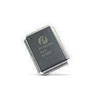
PI7C7300DNAE Pericom Semiconductor, PI7C7300DNAE Datasheet - Page 99

PI7C7300DNAE
Manufacturer Part Number
PI7C7300DNAE
Description
IC PCI-PCI BRIDGE 3PORT 272-BGA
Manufacturer
Pericom Semiconductor
Datasheet
1.PI7C7300DNAE.pdf
(107 pages)
Specifications of PI7C7300DNAE
Applications
*
Interface
*
Voltage - Supply
*
Package / Case
272-PBGA
Mounting Type
Surface Mount
Maximum Operating Temperature
+ 85 C
Minimum Operating Temperature
- 40 C
Mounting Style
SMD/SMT
Operating Supply Voltage
3 V to 3.6 V
Supply Current (max)
660 mA
Lead Free Status / RoHS Status
Lead free / RoHS Compliant
Available stocks
Company
Part Number
Manufacturer
Quantity
Price
Company:
Part Number:
PI7C7300DNAE
Manufacturer:
Pericom
Quantity:
135
Company:
Part Number:
PI7C7300DNAE
Manufacturer:
MAX
Quantity:
5 510
16.2
16.3
Pericom Semiconductor
Table 16-1 TAP PINS
Upon activation of the TRST# reset pin, the latched instruction asynchronously changes
to the id code instruction. When the TAP controller moves into the test state other than
by reset activation, the opcode changes as TDI shifts, and becomes active on the falling
edge of TCK.
BOUNDARY-SCAN INSTRUCTION SET
The PI7C7300D supports three mandatory boundary-scan instructions (bypass,
sample/preload and extest). The table shown below lists the PI7C7300D’s boundary-scan
instruction codes. The “reserved” code should not be used.
TAP TEST DATA REGISTERS
The PI7C7300D contains two test data registers (bypass and boundary-scan). Each test
data register selected by the TAP controller is connected serially between TDI and TDO.
TDI is connected to the test data register’s most significant bit. TDO is connected to the
least significant bit. Data is shifted one bit position within the register towards TDO on
Instruction Code
(binary)
0000
0001
Instruction
Requisite
Extest
IEEE 1149.1
Required
Sample/preload
IEEE 1149.1
Required
Idcode
IEEE 1149.1
Required
Bypass
IEEE 1149.1
Required
/
Opcode (binary)
0000
0001
0101
1111
Instruction Name
EXTEST
SAMPLE/PRELOAD
Page 99 of 107
1. A snapshot of the sample instruction is captured on the rising
Extest initiates testing of external circuitry, typically board-level
Bypass instruction selects the one-bit bypass register between
Description
interconnects and off chip circuitry. Extest connects the
boundary-scan register between TDI and TDO. When Extest is
selected, all output signal pin values are driven by values shifted
into the boundary-scan register and may change only of the
falling edge of TCK. Also, when extest is selected, all system
input pin states must be loaded into the boundary-scan register on
the rising-edge of TCK.
Sample/preload performs two functions:
2. On the falling edge of TCK, the data held in the boundary-scan
Reserved
TDI and TDO pins. 0 (binary) is the only instruction that
accesses the bypass register. While this instruction is in effect,
all other test data registers have no effect on system operation.
Test data registers with both test and system functionality
perform their system functions when this instruction is selected.
edge of TCK without interfering with normal operation. The
instruction causes boundary-scan register cells associated with
outputs to sample the value being driven.
cells is transferred to the slave register cells. Typically, the
slave latched data is applied to the system outputs via the
extest instruction.
Instruction Code
(binary)
0101
1111
3-PORT PCI-TO-PCI BRIDGE
November 2005 - Revision 1.01
Instruction Name
Reserved
Bypass
PI7C7300D


