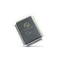
PI7C7300DNAE Pericom Semiconductor, PI7C7300DNAE Datasheet - Page 80

PI7C7300DNAE
Manufacturer Part Number
PI7C7300DNAE
Description
IC PCI-PCI BRIDGE 3PORT 272-BGA
Manufacturer
Pericom Semiconductor
Datasheet
1.PI7C7300DNAE.pdf
(107 pages)
Specifications of PI7C7300DNAE
Applications
*
Interface
*
Voltage - Supply
*
Package / Case
272-PBGA
Mounting Type
Surface Mount
Maximum Operating Temperature
+ 85 C
Minimum Operating Temperature
- 40 C
Mounting Style
SMD/SMT
Operating Supply Voltage
3 V to 3.6 V
Supply Current (max)
660 mA
Lead Free Status / RoHS Status
Lead free / RoHS Compliant
Available stocks
Company
Part Number
Manufacturer
Quantity
Price
Company:
Part Number:
PI7C7300DNAE
Manufacturer:
Pericom
Quantity:
135
Company:
Part Number:
PI7C7300DNAE
Manufacturer:
MAX
Quantity:
5 510
14.1.14
14.1.15
14.1.16
Pericom Semiconductor
I/O BASE REGISTER – OFFSET 1Ch
I/O LIMIT REGISTER – OFFSET 1Ch
SECONDARY STATUS REGISTER – OFFSET 1Ch
Bit
3:0
7:4
Bit
11:8
15:12
Bit
20:16
21
22
23
24
26:25
I/O Base Address
Reserved
66MHz Capable
Reserved
Function
32-bit Indicator
I/O Base Address
[15:12]
Function
32-bit Indicator
[15:12]
Function
Fast Back-to-
Back Capable
Data Parity Error
Detected
DEVSEL#
timing
Type
R/O
R/W
Type
R/O
R/W
Type
R/O
R/O
R/O
R/O
R/WC
R/O
Page 80 of 107
Description
Read as 01h to indicate 32-bit I/O addressing
Defines the bottom address of the I/O address range for the bridge
to determine when to forward I/O transactions from one interface to
the other. The upper 4 bits correspond to address bits [15:12] and
are writable. The lower 12 bits corresponding to address bits [11:0]
are assumed to be 0. The upper 16 bits corresponding to address
bits [31:16] are defined in the I/O base address upper 16 bits address
register
Reset to 0
Description
Read as 01h to indicate 32-bit I/O addressing
Defines the top address of the I/O address range for the bridge to
determine when to forward I/O transactions from one interface to
the other. The upper 4 bits correspond to address bits [15:12] and
are writable. The lower 12 bits corresponding to address bits [11:0]
are assumed to be FFFh. The upper 16 bits corresponding to
address bits [31:16] are defined in the I/O base address upper 16 bits
address register
Reset to 0
Description
Reset to 0
Set to 1 to enable 66MHz operation on the secondary (S1 or S2)
interface
Reset to 1
Reset to 0
Set to 1 to enable decoding of fast back-to-back transactions on the
secondary (S1 or S2) interface to different targets
Reset to 0
Set to 1 when S1_PERR# or S2_PERR# is asserted and bit 6 of
command register is set
Reset to 0
DEVSEL# timing (medium decoding)
00: fast DEVSEL# decoding
01: medium DEVSEL# decoding
10: slow DEVSEL# decoding
11: reserved
Reset to 01
3-PORT PCI-TO-PCI BRIDGE
November 2005 - Revision 1.01
PI7C7300D


