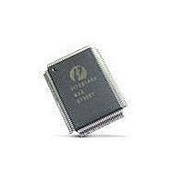
PI7C7300DNAE Pericom Semiconductor, PI7C7300DNAE Datasheet - Page 98

PI7C7300DNAE
Manufacturer Part Number
PI7C7300DNAE
Description
IC PCI-PCI BRIDGE 3PORT 272-BGA
Manufacturer
Pericom Semiconductor
Datasheet
1.PI7C7300DNAE.pdf
(107 pages)
Specifications of PI7C7300DNAE
Applications
*
Interface
*
Voltage - Supply
*
Package / Case
272-PBGA
Mounting Type
Surface Mount
Maximum Operating Temperature
+ 85 C
Minimum Operating Temperature
- 40 C
Mounting Style
SMD/SMT
Operating Supply Voltage
3 V to 3.6 V
Supply Current (max)
660 mA
Lead Free Status / RoHS Status
Lead free / RoHS Compliant
Available stocks
Company
Part Number
Manufacturer
Quantity
Price
Company:
Part Number:
PI7C7300DNAE
Manufacturer:
Pericom
Quantity:
135
Company:
Part Number:
PI7C7300DNAE
Manufacturer:
MAX
Quantity:
5 510
16.1.1
16.1.2
Pericom Semiconductor
Figure 16-1 TEST ACCESS PORT BLOCK DIAGRAM
TAP PINS
The PI7C7300D’s TAP pins form a serial port composed of four input connections
(TMS, TCK, TRST# and TDI) and one output connection (TDO). These pins are
described in Table 16-1. The TAP pins provide access to the instruction register and the
test data registers.
INSTRUCTION REGISTER
The Instruction Register (IR) holds instruction codes. These codes are shifted in through
the Test Data Input (TDI) pin. The instruction codes are used to select the specific test
operation to be performed and the test data register to be accessed.
The instruction register is a parallel-loadable, master/slave-configured 4-bit wide, serial-
shift register with latched outputs. Data is shifted into and out of the IR serially through
the TDI pin clocked by the rising edge of TCK. The shifted-in instruction becomes active
upon latching from the master stage to the slave stage. At that time the IR outputs along
with the TAP finite state machine outputs are decoded to select and control the test data
register selected by that instruction. Upon latching, all actions caused by any previous
instructions terminate.
The instruction determines the test to be performed, the test data register to be accessed,
or both. The IR is two bits wide. When the IR is selected, the most significant bit is
connected to TDI, and the least significant bit is connected to TDO. The value presented
on the TDI pin is shifted into the IR on each rising edge of TCK. The TAP controller
captures fixed parallel data (1101 binary). When a new instruction is shifted in through
TDI, the value 1101(binary) is always shifted out through TDO, least significant bit first.
This helps identify instructions in a long chain of serial data from several devices.
Page 98 of 107
3-PORT PCI-TO-PCI BRIDGE
November 2005 - Revision 1.01
PI7C7300D


