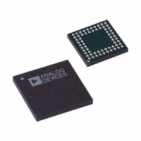
AD9929BBCZ Analog Devices Inc, AD9929BBCZ Datasheet - Page 5

AD9929BBCZ
Manufacturer Part Number
AD9929BBCZ
Description
IC CCD SIGNAL PROCESSOR 64-BGA
Manufacturer
Analog Devices Inc
Type
CCD Signal Processor, 12-Bitr
Datasheet
1.AD9929BBCZ.pdf
(64 pages)
Specifications of AD9929BBCZ
Input Type
Logic
Output Type
Logic
Interface
3-Wire Serial
Mounting Type
Surface Mount
Package / Case
64-CSPBGA
Analog Front End Type
CCD
Analog Front End Category
Video
Interface Type
Serial (3-Wire)
Input Voltage Range
0.5V
Operating Supply Voltage (min)
2.7V
Operating Supply Voltage (typ)
3V
Operating Supply Voltage (max)
3.6V
Resolution
12b
Number Of Adc's
1
Power Supply Type
Analog/Digital
Operating Temp Range
-20C to 85C
Operating Temperature Classification
Commercial
Mounting
Surface Mount
Pin Count
64
Package Type
CSPBGA
Number Of Channels
1
Lead Free Status / RoHS Status
Lead free / RoHS Compliant
Current - Supply
-
Lead Free Status / RoHS Status
Compliant, Lead free / RoHS Compliant
Available stocks
Company
Part Number
Manufacturer
Quantity
Price
Company:
Part Number:
AD9929BBCZ
Manufacturer:
ADI
Quantity:
531
TIMING SPECIFICATIONS
Table 4. C
Parameter
MASTER CLOCK, CLI
AFE CLAMP PULSES
AFE SAMPLE LOCATION
DATA OUTPUTS
SERIAL INTERFACE (See Figure 10 and Figure 11)
1
VERTICAL DRIVER SPECIFICATIONS
Table 5. V1 to V4 load = no load, SUBCK load = no load, VDD = 3.0 V, VL = −7.5 V, VH1 = VH2 = +15.0 V, VM1 = VM2 = GND,
f
Parameter
LOGIC INPUTS
Propagation Delays, Rise/Fall Times and Output Currents
V1 and V3 Outputs (See Figure 43)
CLI
Parameter is programmable.
CLI Clock Period
CLI High/Low Pulse Width
Delay from CLI Rising Edge to Internal Pixel Position 0
CLPOB Pulse Width
SHP Sample Edge to SHD Sample Edge
Output Delay from DCLK1 Rising Edge (See Figure 19)
Pipeline Delay from SHP/SHD Sampling (See Figure 70)
Maximum SCK Frequency
SL to SCK Setup Time
SCK to SL Hold Time
SDATA Valid to SCK Rising Edge Setup
SCK Falling Edge to SDATA Valid Hold
SCK Falling Edge to SDATA Valid Read
High Level Input Voltage
Low Level Input Voltage
Delay Times
Rise Times
Fall Times
Output Currents
= 36 MHz, unless otherwise noted.
VL to VM1
VM1 to VH1
VH1 to VM1
VM1 to VL
VL to VM1
VM1 to VH1
VH1 to VM1
VM1 to VL
V1 or V3 @ VL = −7.25 V
V1 or V3 @ VM1 = −0.25 V
V1 or V3 @ VM1 = +0.25 V
V1 or V3 @ VH1 = +14.75 V
L
= 20 pF, AVDD = DVDD = DRVDD = 3.0 V, f
1
1
(See Figure 17)
CLI
Rev. A | Page 5 of 64
= 36 MHz, unless otherwise noted.
Symbol
V
V
t
t
t
t
t
t
t
t
PLM1
PMH
PHM
PML1
R1
R2
F1
F2
IH
IL
Min
0.8 (VDD)
0
Symbol
t
t
T
t
t
f
t
t
t
t
t
CONV
CLIDLY
OD
DV
SCLK
LS
LH
DS
DH
OD
S1
Min
27.8
4
20
10
10
10
10
10
10
Typ
0.3 (VDD)
100
100
50
50
500
500
500
500
10.0
−5.0
5.0
−7.2
Typ
13.9
6
10
25
9
Max
9
Max
VDD
V
AD9929
Unit
ns
ns
ns
Pixels
Pixels
ns
Cycles
MHz
ns
ns
ns
ns
ns
mA
Unit
V
ns
ns
ns
ns
ns
ns
ns
ns
mA
mA
mA


