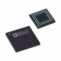
AD9929BBCZ Analog Devices Inc, AD9929BBCZ Datasheet - Page 14

AD9929BBCZ
Manufacturer Part Number
AD9929BBCZ
Description
IC CCD SIGNAL PROCESSOR 64-BGA
Manufacturer
Analog Devices Inc
Type
CCD Signal Processor, 12-Bitr
Datasheet
1.AD9929BBCZ.pdf
(64 pages)
Specifications of AD9929BBCZ
Input Type
Logic
Output Type
Logic
Interface
3-Wire Serial
Mounting Type
Surface Mount
Package / Case
64-CSPBGA
Analog Front End Type
CCD
Analog Front End Category
Video
Interface Type
Serial (3-Wire)
Input Voltage Range
0.5V
Operating Supply Voltage (min)
2.7V
Operating Supply Voltage (typ)
3V
Operating Supply Voltage (max)
3.6V
Resolution
12b
Number Of Adc's
1
Power Supply Type
Analog/Digital
Operating Temp Range
-20C to 85C
Operating Temperature Classification
Commercial
Mounting
Surface Mount
Pin Count
64
Package Type
CSPBGA
Number Of Channels
1
Lead Free Status / RoHS Status
Lead free / RoHS Compliant
Current - Supply
-
Lead Free Status / RoHS Status
Compliant, Lead free / RoHS Compliant
Available stocks
Company
Part Number
Manufacturer
Quantity
Price
Company:
Part Number:
AD9929BBCZ
Manufacturer:
ADI
Quantity:
531
AD9929
Table 9. System Register Address Map (Address 0x14)
Register
Sys_Reg(0)
Sys_Reg(1)
Sys_Reg(2)
Sys_Reg(3)
Sys_Reg(4)
Sys_Reg(5)
Sys_Reg(6)
Sys_Reg(7)
Sys_Reg(8)
Content
(31:24)
(23:0)
(31:23)
22
21
20
19
(18:10)
(9:1)
0
(31:24)
(23:15)
(14:6)
(5:0)
(31:29)
(28:20)
(19:11)
(10:2)
1
0
31
30
(29:21)
(20:12)
(11:3)
(2:0)
(31:26)
(25:17)
(16:8)
(7:0)
31
(30:22)
(21:13)
12
11
10
9
(8:0)
(31:23)
(22:14)
(13:5)
(4:0)
(31:28)
(27:19)
(18:10)
(9:1)
0
Bit
Width
8
24
9
1
1
1
1
9
9
1
8
9
9
6
3
9
9
9
1
1
1
1
9
9
9
3
6
9
9
8
1
9
9
1
1
1
1
9
9
9
9
5
4
9
9
9
1
Default
(Decimal)
NA
NA
37
0
0
1
1
0
19
0
12
31
0
19
12
31
104
0
0
1
1
18
58
47
96
0
76
38
105
57
0
0
1
1
0
29
19
48
0
29
19
48
–
Register Name
System_Reg_addr
System_Number_N
VTPLEN0
XV1STARTPOL0
XV2STARTPOL0
XV3STARTPOL0
XV4STARTPOL0
XV1TOG1POS0
XV1TOG2POS0 Vertical
Sequence
XV2TOG1POS0 [8]
XV2TOG1POS0 [7:0]
XV2TOG2POS0
XV3TOG1POS0
XV3TOG2POS0 [8:3]
XV3TOG2POS0 [2:0]
XV4TOG1POS0
XV4TOG2POS0
VTPLEN1
XV1STARTPOL1
XV2STARTPOL1
XV3STARTPOL1
XV4STARTPOL1
XV1TOG1POS1
XV1TOG2POS1
XV2TOG1POS1
XV2TOG2POS1 [8:6]
XV2TOG2POS1 [5:0]
XV3TOG1POS1
XV3TOG2POS1
XV4TOG1POS1 [8:1]
XV4TOG1POS1 [0]
XV4TOG2POS1
VTPLEN2
XV1STARTPOL2
XV2STARTPOL2
XV3STARTPOL2
XV4STARTPOL2
XV1TOG1POS2
XV1TOG2POS2
XV2TOG1POS2
XV2TOG2POS2
XV3TOG1POS2 [8:4]
XV3TOG1POS2 [3:0]
XV3TOG2POS2
XV4TOG1POS2
XV4TOG2POS2
Unused
Rev. A | Page 14 of 64
Register Description
System Register Address is (Address 0x14)
Number N Register Writes (0x000000 = Write All
Registers)
Vertical Sequence #0: Length Between Repetitions
Vertical Sequence #0: XV1 Start Polarity
Vertical Sequence #0: XV2 Start Polarity
Vertical Sequence #0: XV3 Start Polarity
Vertical Sequence #0: XV4 Start Polarity
Vertical Sequence #0: XV1 Toggle Position 1
#0: XV1 Toggle Position 2
Vertical Sequence #0: XV2 Toggle Position 1
Vertical Sequence #0: XV2 Toggle Position 2
Vertical Sequence #0: XV3 Toggle Position 1
Vertical Sequence #0: XV3 Toggle Position 2
Vertical Sequence #0: XV4 Toggle Position 1
Vertical Sequence #0: XV4 Toggle Position 2
Vertical Sequence #1: Length Between Repetitions
Vertical Sequence #1: XV1 Start Polarity
Vertical Sequence #1: XV2 Start Polarity
Vertical Sequence #1: XV3 Start Polarity
Vertical Sequence #1: XV4 Start Polarity
Vertical Sequence #1: XV1 Toggle Position 1
Vertical Sequence #1: XV1 Toggle Position 2
Vertical Sequence #1: XV2 Toggle Position 1
Vertical Sequence #1: XV2Toggle Position 2
Vertical Sequence #1: XV3 Toggle Position 1
Vertical Sequence #1: XV3 Toggle Position 2
Vertical Sequence #1: XV4 Toggle Position 1
Vertical Sequence #1: XV4 Toggle Position 2
Vertical Sequence #2: Length between Repetitions
Vertical Sequence #2: XV1 Start Polarity
Vertical Sequence #2: XV2 Start Polarity
Vertical Sequence #2: XV3 Start Polarity
Vertical Sequence #2: XV4 Start Polarity
Vertical Sequence #2: XV1 Toggle Position 1
Vertical Sequence #2: XV1 Toggle Position 2
Vertical Sequence #2: XV2 Toggle Position 1
Vertical Sequence #2: XV2 Toggle Position 2
Vertical Sequence #2: XV3 Toggle Position 1
Vertical Sequence #2: XV3 Toggle Position 2
Vertical Sequence #2: XV4 Toggle Position 1
Vertical Sequence #2: XV4 Toggle Position 2


