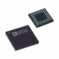
AD9929BBCZ Analog Devices Inc, AD9929BBCZ Datasheet - Page 40

AD9929BBCZ
Manufacturer Part Number
AD9929BBCZ
Description
IC CCD SIGNAL PROCESSOR 64-BGA
Manufacturer
Analog Devices Inc
Type
CCD Signal Processor, 12-Bitr
Datasheet
1.AD9929BBCZ.pdf
(64 pages)
Specifications of AD9929BBCZ
Input Type
Logic
Output Type
Logic
Interface
3-Wire Serial
Mounting Type
Surface Mount
Package / Case
64-CSPBGA
Analog Front End Type
CCD
Analog Front End Category
Video
Interface Type
Serial (3-Wire)
Input Voltage Range
0.5V
Operating Supply Voltage (min)
2.7V
Operating Supply Voltage (typ)
3V
Operating Supply Voltage (max)
3.6V
Resolution
12b
Number Of Adc's
1
Power Supply Type
Analog/Digital
Operating Temp Range
-20C to 85C
Operating Temperature Classification
Commercial
Mounting
Surface Mount
Pin Count
64
Package Type
CSPBGA
Number Of Channels
1
Lead Free Status / RoHS Status
Lead free / RoHS Compliant
Current - Supply
-
Lead Free Status / RoHS Status
Compliant, Lead free / RoHS Compliant
Available stocks
Company
Part Number
Manufacturer
Quantity
Price
Company:
Part Number:
AD9929BBCZ
Manufacturer:
ADI
Quantity:
531
AD9929
SPECIAL VERTICAL TIMING (SPATS)
The AD9929 provides additional special vertical timing gen-
eration (SPATs), which is applied in the same line as the VSG
pulse. The SPAT timing allows for an additional vertical output
pulse in the VSG line. The additional vertical output pulse can
be applied to either XV1, XV2, XV3 or XV4, according to the
value of the SPATLOGIC register. Table 26 lists the registers
used to generate the SPATs, and Table 27 describes the
SPATLOGIC settings and operation.
Table 26. HD and VD Registers
Register Name
SPAT_EN
SPATLOGIC
XV1SPAT_TOG1
XV1SPAT_TOG2
XV1SPAT_TOG3
XV1SPAT_TOG4
XV2SPAT_TOG1
XV2SPAT_TOG2
XV2SPAT_TOG3
XV2SPAT_TOG4
XV3SPAT_TOG1
XV3SPAT_TOG2
XV3SPAT_TOG3
XV3SPAT_TOG4
XV4SPAT_TOG1
XV4SPAT_TOG2
XV4SPAT_TOG3
XV4SPAT_TOG4
XV1SPAT_TOG1
XV1SPAT_TOG2
XV1SPAT_TOG3
XV1SPAT_TOG4
Bit
Width
1
4
13
13
13
13
13
13
13
13
13
13
13
13
13
13
13
13
13
13
13
13
Register Type
Control (Address 0x01)
Control (Address 0x0A)
Control (Address 0x17)
Control (Address 0x18)
Mode_A_Reg(5)
Mode_A_Reg(5)
Control (Address 0x19)
Control (Address 0x1A)
Mode_A_Reg(5)
Mode_A_Reg(5)
Control (Address 0x1B)
Control (Address 0x1C)
Mode_A_Reg(5)
Mode_A_Reg(5)
Control (Address 0x1D)
Control (Address 0x1E)
Mode_A_Reg(5)
Mode_A_Reg(5)
Control (Address 0x1F)
Control (Address 0x20)
Mode_B_Reg(5)
Mode_B_Reg(5)
Reference
Counter
–
–
ST
ST
ST
ST
ST
ST
ST
ST
ST
ST
ST
ST
ST
ST
ST
ST
ST
ST
ST
ST
Rev. A | Page 40 of 64
Range (Pixels)
0–8192
0–8192
0–8192
0–8192
0–8192
0–8192
0–8192
0–8192
0–8192
0–8192
0–8192
0–8192
0–8192
0–8192
0–8192
0–8192
0–8192
0–8192
0–8192
0–8192
Figure 39 and Figure 40 show AND and OR SPAT pulse
examples using four SPAT toggle positions. As shown in these
figures, the internal SPAT timing for the AND case initially
starts high and then goes low at the first XVxSPAT_TOG1
position. In the OR case, the internal SPAT timing initially starts
low and then toggles high at the first XVxSPAT_TOG1 position.
This provides the ability to output the second vertical pulse
when the internal XVx pulse is in both high and low states. Note
that although Figure 39 and Figure 40 show four SPAT toggle
positions, two SPAT toggle positions can be applied by setting
XVxSPAT_TOG3 = XVxSPAT_TOG4 = 0x1FFF.
Description
SPAT Enable Control
(0 = SPAT Disabled, 1 = SPAT Enabled)
SPAT Logic Setting
XV1SPAT Toggle Position #1
(Mode_A Active)
XV1SPAT Toggle Position #2
(Mode_A Active)
XV1SPAT Toggle Position #3
(Mode_A Active)
XV1SPAT Toggle Position #4
(Mode_A Active)
XV2SPAT Toggle Position #1
(Mode_A Active)
XV2SPAT Toggle Position #2
(Mode_A Active)
XV2SPAT Toggle Position #3
(Mode_A Active)
XV2SPAT Toggle Position #4
(Mode_A Active)
XV3SPAT Toggle Position #1
(Mode_A Active)
XV3SPAT Toggle Position #2
(Mode_A Active)
XV3SPAT Toggle Position #3
(Mode_A Active)
XV3SPAT Toggle Position #4
(Mode_A Active)
XV4SPAT Toggle Position #1
(Mode_A Active)
XV4SPAT Toggle Position #2
(Mode_A Active)
XV4SPAT Toggle Position #3
(Mode_A Active)
XV4SPAT Toggle Position #4
(Mode_A Active)
XV1SPAT Toggle Position #1
(Mode_B Active)
XV1SPAT Toggle Position #2
(Mode_B Active)
XV1SPAT Toggle Position #3
(Mode_B Active)
XV1SPAT Toggle Position #4
(Mode_B Active)


