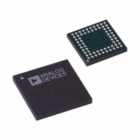
AD9929BBCZ Analog Devices Inc, AD9929BBCZ Datasheet - Page 33

AD9929BBCZ
Manufacturer Part Number
AD9929BBCZ
Description
IC CCD SIGNAL PROCESSOR 64-BGA
Manufacturer
Analog Devices Inc
Type
CCD Signal Processor, 12-Bitr
Datasheet
1.AD9929BBCZ.pdf
(64 pages)
Specifications of AD9929BBCZ
Input Type
Logic
Output Type
Logic
Interface
3-Wire Serial
Mounting Type
Surface Mount
Package / Case
64-CSPBGA
Analog Front End Type
CCD
Analog Front End Category
Video
Interface Type
Serial (3-Wire)
Input Voltage Range
0.5V
Operating Supply Voltage (min)
2.7V
Operating Supply Voltage (typ)
3V
Operating Supply Voltage (max)
3.6V
Resolution
12b
Number Of Adc's
1
Power Supply Type
Analog/Digital
Operating Temp Range
-20C to 85C
Operating Temperature Classification
Commercial
Mounting
Surface Mount
Pin Count
64
Package Type
CSPBGA
Number Of Channels
1
Lead Free Status / RoHS Status
Lead free / RoHS Compliant
Current - Supply
-
Lead Free Status / RoHS Status
Compliant, Lead free / RoHS Compliant
Available stocks
Company
Part Number
Manufacturer
Quantity
Price
Company:
Part Number:
AD9929BBCZ
Manufacturer:
ADI
Quantity:
531
VGATE MASKING OF XV1 TO XV4 AND CLPOB OUTPUTS
During slave mode operation, the SYNC/VGATE Pin 45 is
configured as an input for an external VGATE signal. While
operating in this mode, the external VGATE signal can be used
to mask the XV1 to XV4 and CLPOB outputs. There are two
options available for masking the XV1 to XV4 and CLPOB
outputs. These options are determined by the setting of the
MSHUT/VGATE_EN register located at Control Address 0x01.
Examples of these two options are shown in Figure 30 and
Figure 31. Figure 30 shows MSHUT/VGATE_EN = 0. In this
example, the VGATE signal is internally latched on the falling
(INTERNAL)
(INTERNAL)
(PIN #45)
XV1–XV4
(PIN #45)
XV1–XV4
CLPOB
MSHUT
CLPOB
VGATE
VGATE
VGATE
VGATE
HD
VD
VD
HD
Figure 30. Example of VGATE Input Masking V1 to V4 and CLPOB Outputs with MSHUT/VGATE_EN = 0
Figure 31. Example of VGATE Input Masking V1to V4 and CLPOB Outputs with MSHUT/VGATE_EN = 1
XV1–XV4 AND CLPOB MASKED
Rev. A | Page 33 of 64
edge of HD, resulting with the XV1 to XV4 and CLPOB outputs
being masked when the internally latched VGATE signal is
high.
Figure 31 shows MSHUT/VGATE_EN = 1. In this example, the
preprogrammed MSHUT signal blocks the VGATE input from
masking XV1 to XV4 and CLPOB outputs while MSHUT is low.
The internally latched VGATE signal only masks XV1 to XV4
and CLPOB when MSHUT is high, while operating in this
mode.
XV1–XV4 AND CLPOB MASKED
XV1–XV4 AND CLPOB MASKED
AD9929


