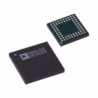
AD9929BBCZ Analog Devices Inc, AD9929BBCZ Datasheet - Page 43

AD9929BBCZ
Manufacturer Part Number
AD9929BBCZ
Description
IC CCD SIGNAL PROCESSOR 64-BGA
Manufacturer
Analog Devices Inc
Type
CCD Signal Processor, 12-Bitr
Datasheet
1.AD9929BBCZ.pdf
(64 pages)
Specifications of AD9929BBCZ
Input Type
Logic
Output Type
Logic
Interface
3-Wire Serial
Mounting Type
Surface Mount
Package / Case
64-CSPBGA
Analog Front End Type
CCD
Analog Front End Category
Video
Interface Type
Serial (3-Wire)
Input Voltage Range
0.5V
Operating Supply Voltage (min)
2.7V
Operating Supply Voltage (typ)
3V
Operating Supply Voltage (max)
3.6V
Resolution
12b
Number Of Adc's
1
Power Supply Type
Analog/Digital
Operating Temp Range
-20C to 85C
Operating Temperature Classification
Commercial
Mounting
Surface Mount
Pin Count
64
Package Type
CSPBGA
Number Of Channels
1
Lead Free Status / RoHS Status
Lead free / RoHS Compliant
Current - Supply
-
Lead Free Status / RoHS Status
Compliant, Lead free / RoHS Compliant
Available stocks
Company
Part Number
Manufacturer
Quantity
Price
Company:
Part Number:
AD9929BBCZ
Manufacturer:
ADI
Quantity:
531
V1 TO V4 AND SUBCK OUTPUT POLARITIES
As shown in Figure 41, the XV1 to XV4 and XSUBCK are
output signals from the AD9929 timing generator, whereas the
V1 to V1 and SUBCK are output signals from the AD9929
vertical driver. The V1 to V4 and SUBCK polarities are not the
same as the internal XV1 to XV4 and XSUBCK polarities
configured by the AD9929 registers. Table 28 through Table 32
describe the output polarities for these signals versus their input
levels. These tables must be referred to when determining the
register settings for the desired output levels. Figure 46 shows an
example of the V3 output.
Table 28. V1 Output Polarity
XV1
L
L
H
H
Table 29. V2 Output Polarity
V-Driver Input
XV2
L
H
Table 30. SUBCK Output Polarity
V-Driver Input
XSUBCK
L
H
XVSG3
XVSG1
XV1
XV3
V1
V3
V-Driver Input
XVSG1
L
H
L
H
t
PLM1
10%
50%
t
R1
SUBCK Output
VH2
VL
V2 Output
VM2
VL
V1 Output
VH1
VM1
VL
VL
90%
t
10%
50%
PMH
Figure 42. V1 and V3 Transmission Delays and Rise Times
t
R2
90%
Rev. A | Page 43 of 64
Table 31. V3 Output Polarity
V-Driver Input
XV3
L
L
H
H
Table 32. V4 Output Polarity
V-Driver Input
XV4
L
H
t
90%
PHM
GENERATOR
50%
TIMING
t
F1
Figure 41. Internal XV1 to XV4 and XSUBCK Signals
XV1
XVSG1
XV2
XV3
XVSG2
XV4
XSUBCK
XVSG2
L
H
L
H
10%
t
PML1
90%
50%
t
F2
V-DRIVER
LOGIC
V3 Output
VH1
VM1
VL
VL
10%
V-DRIVER
V4 Output
VM2
VL
V-DRIVER
BUFFERS
AD9929
VH1
VM1
VL
V1
V2
V3
V4
SUBCK


