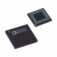
AD9929BBCZ Analog Devices Inc, AD9929BBCZ Datasheet - Page 29

AD9929BBCZ
Manufacturer Part Number
AD9929BBCZ
Description
IC CCD SIGNAL PROCESSOR 64-BGA
Manufacturer
Analog Devices Inc
Type
CCD Signal Processor, 12-Bitr
Datasheet
1.AD9929BBCZ.pdf
(64 pages)
Specifications of AD9929BBCZ
Input Type
Logic
Output Type
Logic
Interface
3-Wire Serial
Mounting Type
Surface Mount
Package / Case
64-CSPBGA
Analog Front End Type
CCD
Analog Front End Category
Video
Interface Type
Serial (3-Wire)
Input Voltage Range
0.5V
Operating Supply Voltage (min)
2.7V
Operating Supply Voltage (typ)
3V
Operating Supply Voltage (max)
3.6V
Resolution
12b
Number Of Adc's
1
Power Supply Type
Analog/Digital
Operating Temp Range
-20C to 85C
Operating Temperature Classification
Commercial
Mounting
Surface Mount
Pin Count
64
Package Type
CSPBGA
Number Of Channels
1
Lead Free Status / RoHS Status
Lead free / RoHS Compliant
Current - Supply
-
Lead Free Status / RoHS Status
Compliant, Lead free / RoHS Compliant
Available stocks
Company
Part Number
Manufacturer
Quantity
Price
Company:
Part Number:
AD9929BBCZ
Manufacturer:
ADI
Quantity:
531
HORIZONTAL CLAMPING AND BLANKING
The AD9929’s horizontal clamping and blanking pulses are
programmable to suit a variety of applications. As with the
vertical timing generation, individual sequences are defined for
each signal, which are then organized into multiple regions
during image readout. This allows the dark pixel clamping and
blanking patterns to be changed at each stage of the readout, in
order to accommodate different image transfer timing and high
speed line shifts.
CONTROLLING CLPOB CLAMP PULSE TIMING
The AFE horizontal CLPOB pulse is generated based on the
12-bit gray code counter. Once the length of the 12-bit gray
code counter is set using the HDLEN register (Sys_Reg(12)),
the CLPTOG1 and CLPTOG2 registers (Sys_Reg(15 and 16))
can be used to place the CLPOB pulse location, as shown in
Figure 25. Table 19 lists all CLPOB registers that are used to
configure and control the placement and output of the
CLPOB pulse.
Table 19. CLPOB Registers
Register
Name
CLPOB_CONT
CLPOB_MODE
CLPTOG1
CLPTOG2
CLPEN0
CLPEN1
CLPEN2
CLPEN3
CLPEN4
Bit
Width
1
1
12
12
1
1
1
1
1
Register Type
Control (0x01)
Control (0x01)
Sys_Reg (15)
Sys_Reg
(15 and 16)
Mode_Reg (2)
Mode_Reg (2)
Mode_Reg (2)
Mode_Reg (2)
Mode_Reg (2)
Counter
Reference
–
–
HD
HD
–
–
–
–
–
Rev. A | Page 29 of 64
Range
0 to 4095 pixel
locations
0 to 4095 pixel
locations
The length of the last HD line is set using the HDLASTLEN
register (Sys_Reg(1)). Figure 23 shows how no CLPOB pulse is
asserted when the last HD length set by HDLASTLEN is shorter
than the regular HD length set by HDLEN. Figure 24 shows
how no CLPOB pulse is applied when the last HD length set by
HDLASTLEN is longer than the regular HD length. Note that
the CLPOB pulse is applied in the last line only when
HDLASTLEN = HDLEN.
CLPOB
CLPOB
HD
HD
Description
CLPOB Control (0=CLPOB off, 1 =CLPOB On)
CLPOB CCD Region Control
(0 = Enable CLPENx Register Settings, 1 = Disable
CLPENx Register Settings)
CLPOB Toggle Position 1 (Gray Code Number)
CLPOB Toggle Position 2 (Gray Code Number)
CLPOB Control for CCD Region 0
(0 = CLPOB Disabled, 1 = CLPOB Enabled)
CLPOB Control for CCD Region 1
(0 = CLPOB Disabled, 1 = CLPOB Enabled)
CLPOB Control for CCD Region 2
(0 = CLPOB Disabled, 1 = CLPOB Enabled)
CLPOB Control for CCD Region 3
(0 = CLPOB Disabled, 1 = CLPOB Enabled)
CLPOB Control for CCD Region 4
(0 = CLPOB Disabled, 1 = CLPOB Enabled)
Figure 23. Last HD Shorter than Regular HD
Figure 24. Last HD Longer than Regular HD
LAST LINE
LAST LINE
AD9929


