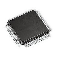
ST92T163R4T1 STMicroelectronics, ST92T163R4T1 Datasheet - Page 93

ST92T163R4T1
Manufacturer Part Number
ST92T163R4T1
Description
Microcontrollers (MCU) OTP EPROM 20K USB/I2
Manufacturer
STMicroelectronics
Datasheet
1.ST92T163R4T1.pdf
(224 pages)
Specifications of ST92T163R4T1
Data Bus Width
8 bit, 16 bit
Program Memory Type
EPROM
Program Memory Size
20 KB
Data Ram Size
2 KB
Interface Type
I2C, SCI, USB
Maximum Clock Frequency
24 MHz
Number Of Programmable I/os
64
Number Of Timers
2
Operating Supply Voltage
4 V to 5.5 V
Maximum Operating Temperature
+ 70 C
Mounting Style
SMD/SMT
Package / Case
TQFP-64
Minimum Operating Temperature
0 C
On-chip Adc
8 bit
Lead Free Status / Rohs Status
No
Available stocks
Company
Part Number
Manufacturer
Quantity
Price
Company:
Part Number:
ST92T163R4T1L
Manufacturer:
ST
Quantity:
444
Part Number:
ST92T163R4T1L
Manufacturer:
ST
Quantity:
20 000
- Current page: 93 of 224
- Download datasheet (2Mb)
EXTERNAL MEMORY SIGNALS (Cont’d)
6.2.4 RW: Read/Write
RW (Alternate Function Output, Active low,
Tristate) identifies the type of memory cycle:
RW=”1” identifies a memory read cycle, RW=”0”
identifies a memory write cycle. It is defined at the
beginning of each memory cycle and it remains
stable until the following memory cycle. RW is re-
leased in high-impedance during bus acknowl-
edge cycle or under processor control by setting
the HIMP bit (MODER). RW is enabled via soft-
ware as the Alternate Function output of the asso-
ciated I/O port bit (refer to specific ST9 device to
identify the port and pin). Under Reset status, the
associated bit of the port is set into bidirectional
weak pull-up mode.
n
n
Figure 52. External memory Read/Write sequence with external wait (WAIT pin)
n
MULTIPLEXED
MULTIPLEXED
ALE (MC=1)
RW (MC=0)
RW (MC=1)
AS (MC=0)
DS (MC=0)
DS (MC=1)
RW (MC=0)
RW (MC=1)
DS (MC=1)
SYST EM
CLOCK
WAI T
P0
P0
P1
ADD.
ADD.
T1
ADDRESS
D.OUT
D.IN
T2
ST92163 - EXTERNAL MEMORY INTERFACE (EXTMI)
ADDRESS
T1
ADDRESS
ADDRESS
The behavior of this signal is affected by the MC,
ETO and BSZ bits in the EMR1 register. Refer to
the Register description.
6.2.5
Acknowledge
Note: These pins are available only on some ST9
devices (see Pin description).
BREQ (Alternate Function Input, Active low) indi-
cates to the ST9 that a bus request has tried or is
trying to gain control of the memory bus. Once en-
abled by setting the BRQEN bit (MODER.1,
R235), BREQ is sampled with the falling edge of
the processor internal clock during phase T2.
D.OUT
D.IN
T2
BREQ,
ADD.
T1
ADD.
BACK:
ADDRESS
Bus
T2
DATA OUT
Request,
D.IN
93/224
Bus
Related parts for ST92T163R4T1
Image
Part Number
Description
Manufacturer
Datasheet
Request
R

Part Number:
Description:
STMicroelectronics [RIPPLE-CARRY BINARY COUNTER/DIVIDERS]
Manufacturer:
STMicroelectronics
Datasheet:

Part Number:
Description:
STMicroelectronics [LIQUID-CRYSTAL DISPLAY DRIVERS]
Manufacturer:
STMicroelectronics
Datasheet:

Part Number:
Description:
BOARD EVAL FOR MEMS SENSORS
Manufacturer:
STMicroelectronics
Datasheet:

Part Number:
Description:
NPN TRANSISTOR POWER MODULE
Manufacturer:
STMicroelectronics
Datasheet:

Part Number:
Description:
TURBOSWITCH ULTRA-FAST HIGH VOLTAGE DIODE
Manufacturer:
STMicroelectronics
Datasheet:

Part Number:
Description:
Manufacturer:
STMicroelectronics
Datasheet:

Part Number:
Description:
DIODE / SCR MODULE
Manufacturer:
STMicroelectronics
Datasheet:

Part Number:
Description:
DIODE / SCR MODULE
Manufacturer:
STMicroelectronics
Datasheet:

Part Number:
Description:
Search -----> STE16N100
Manufacturer:
STMicroelectronics
Datasheet:

Part Number:
Description:
Search ---> STE53NA50
Manufacturer:
STMicroelectronics
Datasheet:

Part Number:
Description:
NPN Transistor Power Module
Manufacturer:
STMicroelectronics
Datasheet:

Part Number:
Description:
DIODE / SCR MODULE
Manufacturer:
STMicroelectronics
Datasheet:


