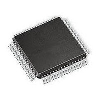
ST92T163R4T1 STMicroelectronics, ST92T163R4T1 Datasheet - Page 102

ST92T163R4T1
Manufacturer Part Number
ST92T163R4T1
Description
Microcontrollers (MCU) OTP EPROM 20K USB/I2
Manufacturer
STMicroelectronics
Datasheet
1.ST92T163R4T1.pdf
(224 pages)
Specifications of ST92T163R4T1
Data Bus Width
8 bit, 16 bit
Program Memory Type
EPROM
Program Memory Size
20 KB
Data Ram Size
2 KB
Interface Type
I2C, SCI, USB
Maximum Clock Frequency
24 MHz
Number Of Programmable I/os
64
Number Of Timers
2
Operating Supply Voltage
4 V to 5.5 V
Maximum Operating Temperature
+ 70 C
Mounting Style
SMD/SMT
Package / Case
TQFP-64
Minimum Operating Temperature
0 C
On-chip Adc
8 bit
Lead Free Status / Rohs Status
No
Available stocks
Company
Part Number
Manufacturer
Quantity
Price
Company:
Part Number:
ST92T163R4T1L
Manufacturer:
ST
Quantity:
444
Part Number:
ST92T163R4T1L
Manufacturer:
ST
Quantity:
20 000
ST92163 - I/O PORTS
INPUT/OUTPUT BIT CONFIGURATION (Cont’d)
When Px.n is programmed as an Output:
(Figure 58)
– The Output Buffer is turned on in an Open-drain
– The data stored in the Output Master Latch is
When Px.n is programmed as Bidirectional:
(Figure 59)
– The Output Buffer is turned on in an Open-Drain
– The data present on the I/O pin is sampled into
– The data stored in the Output Master Latch is
WARNING: Due to the fact that in bidirectional
mode the external pin is read instead of the output
latch, particular care must be taken with arithme-
tic/logic and Boolean instructions performed on a
bidirectional port pin.
These instructions use a read-modify-write se-
quence, and the result written in the port register
depends on the logical level present on the exter-
nal pin.
This may bring unwanted modifications to the port
output register content.
For example:
Port register content, 0Fh
external port value, 03h
(Bits 3 and 2 are externally forced to 0)
A bset instruction on bit 7 will return:
Port register content, 83h
external port value, 83h
(Bits 3 and 2 have been cleared).
To avoid this situation, it is suggested that all oper-
ations on a port, using at least one bit in bidirec-
tional mode, are performed on a copy of the port
register, then transferring the result with a load in-
struction to the I/O port.
When Px.n is programmed as a digital Alter-
nate Function Output:
(Figure 60)
– The Output Buffer is turned on in an Open-Drain
102/224
or Push-pull configuration.
copied both into the Input Latch and into the Out-
put Slave Latch, driving the I/O pin, at the end of
the execution of the instruction.
or Weak Pull-up configuration (except when dis-
abled in hardware).
the Input Latch at the beginning of the execution
of the instruction.
copied into the Output Slave Latch, driving the I/
O pin, at the end of the execution of the instruc-
tion.
or Push-Pull configuration.
– The data present on the I/O pin is sampled into
– The signal from an on-chip function is allowed to
Figure 59. Bidirectional Configuration
n
n
Figure 60. Alternate Function Configuration
n
n
n
n
n
n
the Input Latch at the beginning of the execution
of the instruction.
load the Output Slave Latch driving the I/O pin.
Signal timing is under control of the alternate
function. If no alternate function is connected to
Px.n, the I/O pin is driven to a high level when in
Push-Pull configuration, and to a high imped-
ance state when in open drain configuration.
WEAK PULL-UP
OPEN DRAIN
OPEN DRAIN
PUSH-PULL
PERIPHERAL
OUTPUT MASTER LATCH
OUTPUT SLAVE LATCH
OUTPUT
OUTPUT SLAVE LATCH
FROM
INTERNAL DATA BUS
INTERNAL DATA BUS
I/O PIN
I/O PIN
INPUT LATCH
INPUT LATCH
(or Schmitt Trigger)
(or Schmitt Trigger)
TO PERIPHERAL
INTERRUPTS
INPUTS AND
TO PERIPHERAL
INTERRUPTS
INPUTS AND
TTL
TTL


